

Consulte las especificaciones para obtener detalles del producto.
LTC1322CN#PBF
Product Overview
Category: Integrated Circuit (IC)
Use: The LTC1322CN#PBF is a versatile integrated circuit primarily used for signal conditioning and data acquisition applications. It is commonly employed in various electronic systems to amplify, filter, and convert analog signals.
Characteristics: - High precision and accuracy - Low power consumption - Wide operating voltage range - Excellent noise performance - Compact size and lightweight - Robust and reliable
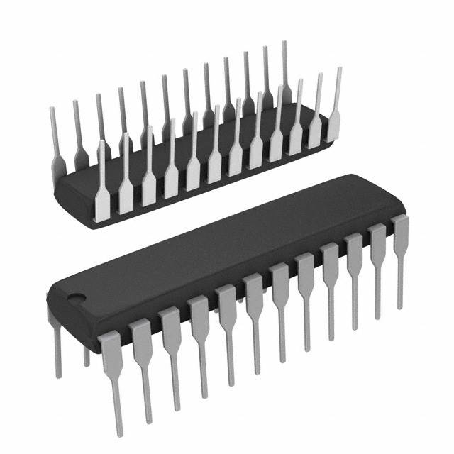
Package: The LTC1322CN#PBF is available in a 16-pin plastic DIP (Dual Inline Package) format. This package offers ease of handling and compatibility with standard PCB (Printed Circuit Board) designs.
Essence: The essence of the LTC1322CN#PBF lies in its ability to enhance the quality and reliability of analog signals in electronic systems. By providing precise signal conditioning and data acquisition capabilities, it enables accurate measurement and control in various applications.
Packaging/Quantity: The LTC1322CN#PBF is typically supplied in tape and reel packaging, ensuring safe transportation and convenient handling during manufacturing processes. The quantity per reel varies depending on the manufacturer's specifications.
Specifications
- Supply Voltage Range: 2.7V to 5.5V
- Operating Temperature Range: -40°C to 85°C
- Analog Input Voltage Range: ±10V
- Resolution: 12 bits
- Sampling Rate: Up to 100 kSPS (thousand samples per second)
- Total Harmonic Distortion (THD): <0.01%
- Power Consumption: <1mW
Pin Configuration
The LTC1322CN#PBF features a 16-pin configuration as follows:
- VREF- (Reference Voltage Negative Input)
- VREF+ (Reference Voltage Positive Input)
- AGND (Analog Ground)
- IN1 (Analog Input 1)
- IN2 (Analog Input 2)
- IN3 (Analog Input 3)
- IN4 (Analog Input 4)
- OUT1 (Analog Output 1)
- OUT2 (Analog Output 2)
- SCK (Serial Clock Input)
- SDI (Serial Data Input)
- SDO (Serial Data Output)
- CS (Chip Select)
- DGND (Digital Ground)
- VCC (Supply Voltage)
- REFOUT (Reference Output)
Functional Features
- High-resolution analog-to-digital conversion
- Programmable gain amplifier for signal amplification
- Built-in digital filters for noise reduction
- Serial interface for easy integration with microcontrollers and other digital devices
- Flexible power supply options for compatibility with various systems
- On-chip reference voltage generation for accurate measurements
Advantages and Disadvantages
Advantages: - High precision and accuracy enable reliable data acquisition - Low power consumption prolongs battery life in portable applications - Wide operating voltage range enhances versatility - Excellent noise performance ensures clean and reliable signals - Compact size allows for space-efficient designs - Robust construction ensures long-term reliability
Disadvantages: - Limited analog input voltage range may restrict certain applications - Higher cost compared to lower-end signal conditioning ICs - Requires additional external components for complete functionality
Working Principles
The LTC1322CN#PBF operates based on the principles of analog-to-digital conversion and signal conditioning. It utilizes a combination of programmable gain amplifiers, analog-to-digital converters, and digital filters to accurately process analog signals.
When an analog signal is applied to one of the input pins, the LTC1322CN#PBF amplifies and conditions the signal using the programmable gain amplifier. The amplified signal is then converted into a digital representation by the analog-to-digital converter.
The digital data is further processed and filtered to remove noise and unwanted artifacts. The resulting clean and accurate digital signal can be easily interfaced with microcontrollers or other digital devices for further analysis or control.
Detailed Application Field Plans
The LTC1322CN#PBF finds applications in various fields, including but not limited to:
- Industrial Automation: Used for precise measurement and control of analog signals in industrial processes.
- Medical Devices: Enables accurate data acquisition in medical monitoring equipment.
- Test and Measurement Instruments: Provides high-resolution signal conditioning for accurate measurements.
- Communication Systems: Enhances the quality and reliability of analog signals in communication devices.
- Automotive Electronics: Used for sensor signal conditioning and data acquisition in automotive systems.
Detailed and Complete Alternative Models
- LTC1322CS8#PBF: 8-pin SOIC (Small Outline Integrated Circuit) package variant of LTC1322CN#PBF.
- LTC1322IS8#PBF: 8
Enumere 10 preguntas y respuestas comunes relacionadas con la aplicación de LTC1322CN#PBF en soluciones técnicas
Sure! Here are 10 common questions and answers related to the application of LTC1322CN#PBF in technical solutions:
Q: What is LTC1322CN#PBF? A: LTC1322CN#PBF is a specific model number for a component, namely a low-power, dual 12-bit digital-to-analog converter (DAC) manufactured by Linear Technology.
Q: What is the purpose of LTC1322CN#PBF? A: The LTC1322CN#PBF DAC is used to convert digital signals into analog voltages, making it suitable for various applications such as control systems, instrumentation, and communication devices.
Q: What is the operating voltage range of LTC1322CN#PBF? A: The LTC1322CN#PBF operates within a voltage range of +2.7V to +5.5V.
Q: How many channels does LTC1322CN#PBF have? A: LTC1322CN#PBF is a dual-channel DAC, meaning it has two independent output channels.
Q: What is the resolution of LTC1322CN#PBF? A: LTC1322CN#PBF has a resolution of 12 bits, allowing for precise analog voltage outputs.
Q: What is the maximum output voltage range of LTC1322CN#PBF? A: The LTC1322CN#PBF can provide an output voltage range of 0V to Vref, where Vref is the reference voltage supplied to the DAC.
Q: Does LTC1322CN#PBF support internal or external reference voltage? A: LTC1322CN#PBF supports both internal and external reference voltage options, providing flexibility in different applications.
Q: What is the power consumption of LTC1322CN#PBF? A: The power consumption of LTC1322CN#PBF is relatively low, typically around 1mW.
Q: Can LTC1322CN#PBF operate in harsh environments? A: Yes, LTC1322CN#PBF is designed to operate in a wide temperature range and can withstand harsh environmental conditions.
Q: Are there any evaluation boards or development kits available for LTC1322CN#PBF? A: Yes, Linear Technology provides evaluation boards and development kits that include LTC1322CN#PBF, allowing engineers to easily test and integrate the DAC into their designs.
Please note that the answers provided here are general and may vary depending on specific datasheet information and application requirements.