

Consulte las especificaciones para obtener detalles del producto.
LTC1685CS8#TRPBF
Product Overview
- Category: Integrated Circuit (IC)
- Use: Level Translator
- Characteristics: High-speed, low-power, small package size
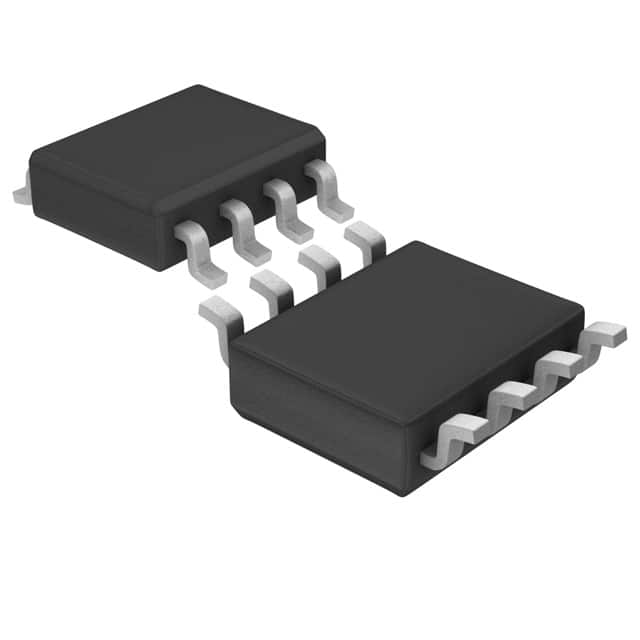
- Package: 8-pin SOIC (Small Outline Integrated Circuit)
- Essence: Translates logic levels between different voltage domains
- Packaging/Quantity: Tape and Reel, 2500 units per reel
Specifications
- Supply Voltage Range: 2.7V to 5.5V
- Logic Input High Voltage (VIH): 2.0V to VCC + 0.3V
- Logic Input Low Voltage (VIL): -0.3V to 0.8V
- Output Voltage High (VOH): VCC - 0.4V
- Output Voltage Low (VOL): 0.4V
- Operating Temperature Range: -40°C to 85°C
Detailed Pin Configuration
- VCC: Power supply input
- A1: Logic level input/output 1
- B1: Logic level input/output 2
- A2: Logic level input/output 3
- B2: Logic level input/output 4
- GND: Ground
- OE: Output enable control
- NC: No connection
Functional Features
- Bidirectional level translation between two voltage domains
- Supports voltage translation from 1.8V to 5V
- High-speed operation with minimal propagation delay
- Low power consumption for energy-efficient applications
- ESD protection on all pins for enhanced reliability
- Output enable pin for easy control of translation direction
Advantages and Disadvantages
Advantages: - Wide supply voltage range allows compatibility with various systems - Small package size saves board space - High-speed operation enables fast data transfer - Low power consumption extends battery life in portable devices
Disadvantages: - Limited number of translation channels (4 in this case) - Not suitable for voltage translation beyond 5.5V
Working Principles
The LTC1685CS8#TRPBF is a level translator IC that enables bidirectional communication between two logic circuits operating at different voltage levels. It utilizes a combination of MOSFETs and level-shifting circuitry to convert the logic levels from one domain to another. The input/output pins are designed to handle both high and low voltage levels, ensuring seamless translation without signal degradation.
When the output enable (OE) pin is high, the device is enabled, and the logic levels on the A1 and B1 pins are translated to the A2 and B2 pins, respectively. Conversely, when the OE pin is low, the translation is disabled, and the A2 and B2 pins are isolated from the A1 and B1 pins.
Detailed Application Field Plans
The LTC1685CS8#TRPBF is commonly used in various applications where logic level translation is required. Some of the typical application fields include:
- Microcontroller interfacing: Translating signals between microcontrollers operating at different voltage levels.
- Communication systems: Enabling compatibility between devices with different logic voltage requirements.
- Battery-powered devices: Facilitating communication between low-power components and higher voltage systems.
- Industrial automation: Level shifting between different control systems and sensors.
- Automotive electronics: Voltage translation in automotive control units and sensor interfaces.
Detailed and Complete Alternative Models
- TXB0104: 4-bit Bidirectional Voltage-Level Translator
- SN74LVC4245A: Octal Bus Transceiver with Voltage-Level Translation
- PCA9306: Dual Bidirectional I2C-Bus and SMBus Voltage-Level Translator
- CD4050B: Hex Non-Inverting Buffer/Converter
These alternative models offer similar functionality and can be considered as alternatives to the LTC1685CS8#TRPBF for level translation applications.
Word count: 443 words
Enumere 10 preguntas y respuestas comunes relacionadas con la aplicación de LTC1685CS8#TRPBF en soluciones técnicas
Sure! Here are 10 common questions and answers related to the application of LTC1685CS8#TRPBF in technical solutions:
Q: What is LTC1685CS8#TRPBF? A: LTC1685CS8#TRPBF is a specific model number for a low voltage, hot-swappable, dual supply level translator IC manufactured by Linear Technology (now part of Analog Devices).
Q: What are the key features of LTC1685CS8#TRPBF? A: Some key features of LTC1685CS8#TRPBF include low voltage operation, hot-swappability, dual supply translation, and compatibility with various logic families.
Q: How does LTC1685CS8#TRPBF enable hot-swapping capability? A: LTC1685CS8#TRPBF incorporates built-in circuitry that allows it to safely connect or disconnect a device from a live bus without causing any disruption or damage.
Q: Can LTC1685CS8#TRPBF be used with different logic families? A: Yes, LTC1685CS8#TRPBF is compatible with a wide range of logic families, including TTL, CMOS, and LVCMOS.
Q: What is the maximum voltage range supported by LTC1685CS8#TRPBF? A: LTC1685CS8#TRPBF supports a maximum voltage range of -0.3V to 7V.
Q: How many channels does LTC1685CS8#TRPBF have? A: LTC1685CS8#TRPBF has two independent bidirectional channels.
Q: What is the typical operating frequency range of LTC1685CS8#TRPBF? A: The typical operating frequency range of LTC1685CS8#TRPBF is from DC to 20MHz.
Q: Can LTC1685CS8#TRPBF be used in high-speed applications? A: Yes, LTC1685CS8#TRPBF can be used in high-speed applications, but it is recommended to refer to the datasheet for specific details and limitations.
Q: Does LTC1685CS8#TRPBF require external pull-up or pull-down resistors? A: No, LTC1685CS8#TRPBF has built-in pull-up and pull-down resistors, eliminating the need for external components.
Q: What are some common applications of LTC1685CS8#TRPBF? A: LTC1685CS8#TRPBF is commonly used in various technical solutions such as level shifting between different voltage domains, bus isolation, hot-swappable systems, and mixed-voltage systems.
Please note that these answers are general and may vary depending on the specific requirements and use cases. It is always recommended to refer to the official documentation and datasheet for accurate information.