

Consulte las especificaciones para obtener detalles del producto.
LTC2630HSC6-HZ10#TRMPBF
Product Overview
Category
The LTC2630HSC6-HZ10#TRMPBF belongs to the category of digital-to-analog converters (DACs).
Use
This product is commonly used in various applications that require high-precision analog voltage generation. It provides a reliable and accurate method for converting digital signals into corresponding analog voltages.
Characteristics
- High precision: The LTC2630HSC6-HZ10#TRMPBF offers exceptional accuracy in generating analog voltages, ensuring precise control in various systems.
- Low power consumption: This DAC is designed to operate efficiently with minimal power consumption, making it suitable for battery-powered devices.
- Wide voltage range: It supports a wide range of output voltage options, allowing flexibility in different applications.
- Fast settling time: The LTC2630HSC6-HZ10#TRMPBF has a fast settling time, enabling rapid response in dynamic systems.
Package
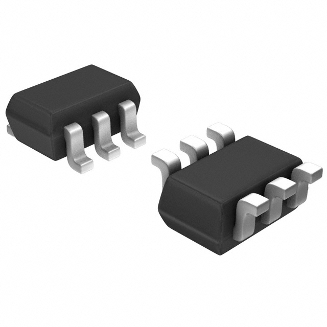
This product comes in a compact HSC-6 package, which ensures easy integration into various circuit designs.
Essence
The essence of the LTC2630HSC6-HZ10#TRMPBF lies in its ability to accurately convert digital signals into precise analog voltages, providing a crucial component for many electronic systems.
Packaging/Quantity
The LTC2630HSC6-HZ10#TRMPBF is typically packaged in reels, containing a specified quantity of units per reel. The exact packaging and quantity can vary depending on the supplier.
Specifications
- Resolution: 10 bits
- Output Voltage Range: 0V to VREF
- Supply Voltage Range: 2.7V to 5.5V
- Operating Temperature Range: -40°C to +85°C
- Interface: SPI-compatible
Detailed Pin Configuration
The LTC2630HSC6-HZ10#TRMPBF has the following pin configuration:
- VDD: Supply voltage input
- GND: Ground reference
- CS: Chip select input
- SCK: Serial clock input
- SDI: Serial data input
- LDAC: Load DAC input
- REF: Reference voltage input
- OUT: Analog output voltage
Functional Features
- High accuracy and resolution for precise analog voltage generation.
- SPI-compatible interface for easy integration with microcontrollers and other digital systems.
- Power-on reset ensures reliable operation upon startup.
- Internal reference voltage for simplified circuit design.
Advantages and Disadvantages
Advantages
- High precision and accuracy in analog voltage generation.
- Low power consumption, suitable for battery-powered devices.
- Wide voltage range provides flexibility in various applications.
- Fast settling time enables rapid response in dynamic systems.
Disadvantages
- Limited resolution compared to higher-bit DACs.
- May require additional external components for specific applications.
Working Principles
The LTC2630HSC6-HZ10#TRMPBF operates by receiving digital input signals through the SPI interface. These digital signals are then converted into corresponding analog voltages using an internal digital-to-analog conversion algorithm. The resulting analog voltage is available at the OUT pin for further use in the system.
Detailed Application Field Plans
The LTC2630HSC6-HZ10#TRMPBF finds application in various fields, including but not limited to: - Industrial automation - Test and measurement equipment - Audio processing systems - Communication devices - Medical instruments
Detailed and Complete Alternative Models
- LTC2630HSC6-HZ12#TRMPBF: 12-bit resolution DAC with similar characteristics and package.
- LTC2630HSC6-HZ8#TRMPBF: 8-bit resolution DAC with similar characteristics and package.
- LTC2630HSC6-HZ16#TRMPBF: 16-bit resolution DAC with similar characteristics and package.
These alternative models provide different resolution options to suit specific application requirements.
Word count: 511 words
Enumere 10 preguntas y respuestas comunes relacionadas con la aplicación de LTC2630HSC6-HZ10#TRMPBF en soluciones técnicas
Sure! Here are 10 common questions and answers related to the application of LTC2630HSC6-HZ10#TRMPBF in technical solutions:
Q: What is LTC2630HSC6-HZ10#TRMPBF? A: LTC2630HSC6-HZ10#TRMPBF is a high-precision, 10-bit digital-to-analog converter (DAC) manufactured by Linear Technology.
Q: What is the operating voltage range of LTC2630HSC6-HZ10#TRMPBF? A: The operating voltage range of LTC2630HSC6-HZ10#TRMPBF is from 2.7V to 5.5V.
Q: What is the resolution of LTC2630HSC6-HZ10#TRMPBF? A: LTC2630HSC6-HZ10#TRMPBF has a resolution of 10 bits, which means it can provide 1024 different output voltage levels.
Q: What is the typical settling time of LTC2630HSC6-HZ10#TRMPBF? A: The typical settling time of LTC2630HSC6-HZ10#TRMPBF is 4.5µs for a full-scale step change.
Q: Can LTC2630HSC6-HZ10#TRMPBF operate in both unipolar and bipolar modes? A: Yes, LTC2630HSC6-HZ10#TRMPBF can operate in both unipolar (0V to Vref) and bipolar (-Vref/2 to +Vref/2) modes.
Q: What is the maximum output current of LTC2630HSC6-HZ10#TRMPBF? A: The maximum output current of LTC2630HSC6-HZ10#TRMPBF is 5mA.
Q: Does LTC2630HSC6-HZ10#TRMPBF have an internal reference voltage? A: No, LTC2630HSC6-HZ10#TRMPBF does not have an internal reference voltage. An external reference voltage must be provided.
Q: Can LTC2630HSC6-HZ10#TRMPBF operate in both single-ended and differential modes? A: Yes, LTC2630HSC6-HZ10#TRMPBF can operate in both single-ended and differential modes.
Q: What is the temperature range for LTC2630HSC6-HZ10#TRMPBF? A: LTC2630HSC6-HZ10#TRMPBF has a temperature range of -40°C to +125°C.
Q: What are some typical applications of LTC2630HSC6-HZ10#TRMPBF? A: LTC2630HSC6-HZ10#TRMPBF is commonly used in applications such as industrial process control, instrumentation, data acquisition systems, and programmable voltage sources.
Please note that these answers are based on general information about LTC2630HSC6-HZ10#TRMPBF and may vary depending on specific use cases and requirements.