

Consulte las especificaciones para obtener detalles del producto.
LTC2637IDE-LZ8#TRPBF
Product Overview
Category
The LTC2637IDE-LZ8#TRPBF belongs to the category of digital-to-analog converters (DACs).
Use
This product is primarily used in applications where a high-precision analog output signal is required. It converts digital data into an analog voltage or current, making it suitable for various industrial and consumer electronic devices.
Characteristics
- High precision: The LTC2637IDE-LZ8#TRPBF offers exceptional accuracy and resolution, ensuring precise analog output.
- Low power consumption: This DAC operates at low power levels, making it energy-efficient and suitable for battery-powered devices.
- Wide operating voltage range: It can operate within a wide voltage range, providing flexibility in different applications.
- Fast settling time: The LTC2637IDE-LZ8#TRPBF has a fast settling time, enabling rapid response in dynamic applications.
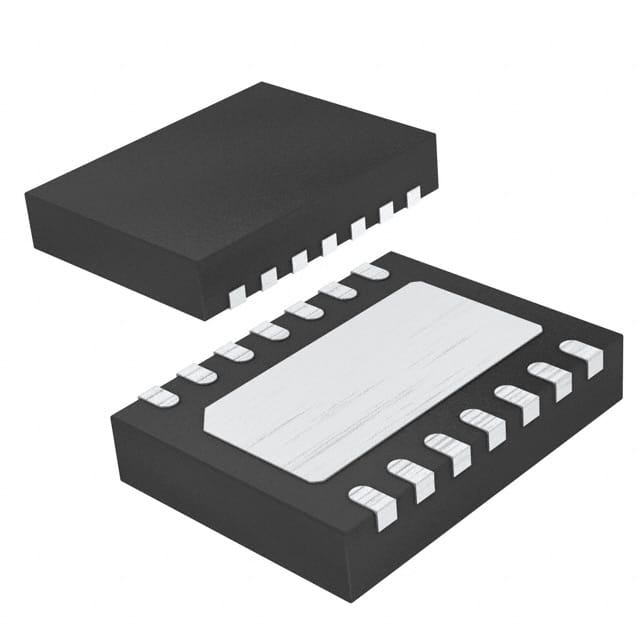
Package
The LTC2637IDE-LZ8#TRPBF comes in a compact and industry-standard package, allowing for easy integration into various circuit designs.
Essence
The essence of this product lies in its ability to convert digital signals into accurate analog outputs, facilitating precise control and measurement in electronic systems.
Packaging/Quantity
The LTC2637IDE-LZ8#TRPBF is typically packaged in reels or tubes, with a quantity of 250 units per reel/tube.
Specifications
- Resolution: 16 bits
- Output type: Voltage or current
- Supply voltage range: 2.7V to 5.5V
- Operating temperature range: -40°C to 85°C
- Interface: SPI-compatible serial interface
- Reference voltage: Internal or external reference options available
Detailed Pin Configuration
The LTC2637IDE-LZ8#TRPBF features a standard pin configuration as follows:
- VDD: Power supply voltage
- GND: Ground reference
- SCK: Serial clock input
- SDI: Serial data input
- LDAC: Load DAC input
- CS: Chip select input
- REF: Reference voltage input
- OUT: Analog output
Functional Features
- High accuracy and resolution for precise analog output.
- Low power consumption, suitable for energy-efficient applications.
- Fast settling time enables rapid response in dynamic systems.
- SPI-compatible serial interface allows for easy integration with microcontrollers and other digital devices.
- Internal or external reference options provide flexibility in different operating conditions.
Advantages and Disadvantages
Advantages
- High precision and resolution ensure accurate analog output.
- Low power consumption makes it suitable for battery-powered devices.
- Wide operating voltage range provides flexibility in various applications.
- Fast settling time enables quick response in dynamic systems.
Disadvantages
- Limited to 16-bit resolution, which may not be sufficient for certain high-precision applications.
- Requires an external reference voltage for optimal performance.
Working Principles
The LTC2637IDE-LZ8#TRPBF operates based on the principle of digital-to-analog conversion. It receives digital input data through the SPI interface and converts it into a corresponding analog voltage or current output. The internal circuitry ensures high accuracy and resolution by utilizing advanced techniques such as digital error correction and calibration.
Detailed Application Field Plans
The LTC2637IDE-LZ8#TRPBF finds application in various fields, including but not limited to: - Industrial automation and control systems - Test and measurement equipment - Audio and video processing devices - Precision instrumentation - Communication systems
Detailed and Complete Alternative Models
- LTC2637A: Similar features and specifications, but with a different package option.
- LTC2637B: Higher resolution (18 bits) version of the LTC2637 series.
- LTC2637C: Lower power consumption variant with reduced operating voltage range.
These alternative models offer different options to suit specific application requirements while maintaining the core functionality of digital-to-analog conversion.
Word count: 536 words
Enumere 10 preguntas y respuestas comunes relacionadas con la aplicación de LTC2637IDE-LZ8#TRPBF en soluciones técnicas
Sure! Here are 10 common questions and answers related to the application of LTC2637IDE-LZ8#TRPBF in technical solutions:
Q: What is LTC2637IDE-LZ8#TRPBF? A: LTC2637IDE-LZ8#TRPBF is a specific model number for a digital-to-analog converter (DAC) chip manufactured by Linear Technology (now part of Analog Devices). It is used to convert digital signals into analog voltages.
Q: What is the purpose of LTC2637IDE-LZ8#TRPBF in technical solutions? A: The LTC2637IDE-LZ8#TRPBF DAC is commonly used in various technical solutions where precise analog voltage outputs are required, such as industrial control systems, instrumentation, test equipment, and communication devices.
Q: What is the resolution of LTC2637IDE-LZ8#TRPBF? A: LTC2637IDE-LZ8#TRPBF has a resolution of 12 bits, which means it can provide 4096 discrete voltage levels between its reference voltage range.
Q: What is the output voltage range of LTC2637IDE-LZ8#TRPBF? A: The output voltage range of LTC2637IDE-LZ8#TRPBF depends on the reference voltage provided to the chip. It can be programmed to output voltages within the range of the reference voltage.
Q: How is LTC2637IDE-LZ8#TRPBF controlled? A: LTC2637IDE-LZ8#TRPBF can be controlled through a serial interface using standard protocols like I2C or SPI. This allows for easy integration with microcontrollers or other digital systems.
Q: Can LTC2637IDE-LZ8#TRPBF operate on a single power supply? A: Yes, LTC2637IDE-LZ8#TRPBF can operate on a single power supply voltage ranging from 2.7V to 5.5V.
Q: Does LTC2637IDE-LZ8#TRPBF have internal reference voltage options? A: Yes, LTC2637IDE-LZ8#TRPBF provides an internal reference voltage option of 2.048V. However, it also supports external reference voltages if more precision or a different voltage range is required.
Q: Can multiple LTC2637IDE-LZ8#TRPBF chips be used together? A: Yes, multiple LTC2637IDE-LZ8#TRPBF chips can be used together in applications that require multiple analog outputs. Each chip can be individually addressed and controlled.
Q: Is LTC2637IDE-LZ8#TRPBF suitable for high-speed applications? A: LTC2637IDE-LZ8#TRPBF is not specifically designed for high-speed applications. It has a settling time of around 10µs, which may limit its use in certain high-frequency applications.
Q: Are evaluation boards available for LTC2637IDE-LZ8#TRPBF? A: Yes, Analog Devices provides evaluation boards for LTC2637IDE-LZ8#TRPBF, which can help users quickly prototype and test their applications before integrating the chip into their final designs.
Please note that the answers provided here are general and may vary depending on specific application requirements and datasheet specifications.