

Consulte las especificaciones para obtener detalles del producto.
LTC2637IMS-LZ8#TRPBF
Product Overview
- Category: Integrated Circuit (IC)
- Use: Digital-to-Analog Converter (DAC)
- Characteristics: High precision, low noise, small package size
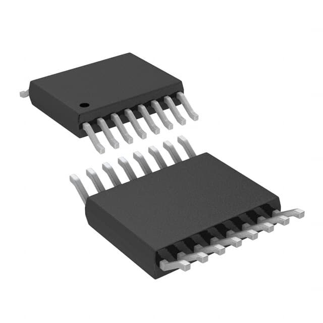
- Package: MSOP-10
- Essence: Converts digital signals into analog voltages
- Packaging/Quantity: Tape & Reel, 2500 units per reel
Specifications
- Resolution: 12 bits
- Number of Channels: 1
- Output Type: Voltage
- Output Range: 0V to VREF
- Reference Voltage Range: 2.5V to 5.5V
- Supply Voltage Range: 2.7V to 5.5V
- Operating Temperature Range: -40°C to +85°C
Detailed Pin Configuration
The LTC2637IMS-LZ8#TRPBF has the following pin configuration:
- VDD: Power supply voltage input
- GND: Ground reference
- SDA: Serial data input
- SCL: Serial clock input
- A0: Address input bit 0
- A1: Address input bit 1
- A2: Address input bit 2
- REF: Reference voltage input
- AGND: Analog ground reference
- OUT: Analog output voltage
Functional Features
- High accuracy and resolution for precise analog voltage generation
- Low noise performance for clean signal generation
- Wide operating temperature range for versatile applications
- Single-channel design for simplicity and cost-effectiveness
- Serial interface for easy integration with microcontrollers or other digital systems
Advantages and Disadvantages
Advantages
- High precision and resolution ensure accurate analog voltage outputs.
- Low noise performance guarantees clean and reliable signal generation.
- Small package size (MSOP-10) allows for space-constrained applications.
- Wide operating temperature range enables usage in various environments.
Disadvantages
- Limited to single-channel output, not suitable for multi-channel applications.
- Requires an external reference voltage source for operation.
Working Principles
The LTC2637IMS-LZ8#TRPBF is a digital-to-analog converter (DAC) that converts digital signals into analog voltages. It utilizes a high-resolution 12-bit architecture to provide precise and accurate analog outputs. The device operates by receiving digital input data through the serial interface (SDA and SCL pins) and converting it into corresponding analog voltage levels at the OUT pin. The reference voltage (VREF) determines the maximum output voltage range, which can be set between 0V and VREF. The DAC's performance is further enhanced by its low noise characteristics, ensuring clean and reliable analog signal generation.
Detailed Application Field Plans
The LTC2637IMS-LZ8#TRPBF finds applications in various fields where accurate analog voltage generation is required. Some potential application areas include:
- Industrial Automation: Precise control of analog actuators and sensors.
- Test and Measurement Equipment: Calibration and signal generation.
- Audio Systems: High-fidelity audio signal processing and amplification.
- Communication Systems: Analog modulation and demodulation circuits.
- Medical Devices: Accurate control of medical equipment and sensors.
Detailed and Complete Alternative Models
- LTC2637A: Similar specifications with additional features such as internal reference voltage.
- MAX5216: 16-bit resolution DAC with similar package size and supply voltage range.
- MCP4921: Low-cost 12-bit DAC with SPI interface and wide supply voltage range.
Note: This is not an exhaustive list, and there are several other alternative models available in the market.
Word count: 408 words
Enumere 10 preguntas y respuestas comunes relacionadas con la aplicación de LTC2637IMS-LZ8#TRPBF en soluciones técnicas
Sure! Here are 10 common questions and answers related to the application of LTC2637IMS-LZ8#TRPBF in technical solutions:
Q: What is LTC2637IMS-LZ8#TRPBF? A: LTC2637IMS-LZ8#TRPBF is a digital-to-analog converter (DAC) manufactured by Linear Technology (now part of Analog Devices). It is a low-power, 12-bit DAC with an integrated reference.
Q: What is the operating voltage range of LTC2637IMS-LZ8#TRPBF? A: The operating voltage range of LTC2637IMS-LZ8#TRPBF is from 2.7V to 5.5V.
Q: What is the resolution of LTC2637IMS-LZ8#TRPBF? A: LTC2637IMS-LZ8#TRPBF has a resolution of 12 bits, which means it can provide 4096 different output voltage levels.
Q: How does LTC2637IMS-LZ8#TRPBF communicate with a microcontroller or other digital devices? A: LTC2637IMS-LZ8#TRPBF uses a standard serial interface called I2C (Inter-Integrated Circuit) to communicate with other devices.
Q: Can LTC2637IMS-LZ8#TRPBF operate in both single-ended and differential modes? A: Yes, LTC2637IMS-LZ8#TRPBF can operate in both single-ended and differential modes, depending on the application requirements.
Q: What is the typical settling time of LTC2637IMS-LZ8#TRPBF? A: The typical settling time of LTC2637IMS-LZ8#TRPBF is 6µs, which refers to the time it takes for the output voltage to stabilize after a change in the digital input.
Q: Can LTC2637IMS-LZ8#TRPBF provide a programmable output voltage range? A: Yes, LTC2637IMS-LZ8#TRPBF allows you to program the output voltage range using its internal reference and gain settings.
Q: What is the power consumption of LTC2637IMS-LZ8#TRPBF? A: The power consumption of LTC2637IMS-LZ8#TRPBF depends on the operating conditions but typically ranges from a few microamps to a few milliamps.
Q: Is LTC2637IMS-LZ8#TRPBF suitable for battery-powered applications? A: Yes, LTC2637IMS-LZ8#TRPBF is designed to operate at low power and can be used in battery-powered applications where power efficiency is crucial.
Q: Are there any evaluation boards or development kits available for LTC2637IMS-LZ8#TRPBF? A: Yes, Analog Devices provides evaluation boards and development kits that include LTC2637IMS-LZ8#TRPBF, allowing engineers to quickly prototype and test their designs.
Please note that the answers provided here are general and may vary depending on specific datasheet specifications and application requirements.