

Consulte las especificaciones para obtener detalles del producto.
MAX13325GUI/V+T
Overview
- Category: Integrated Circuit
- Use: Power Management
- Characteristics: High Efficiency, Low Power Consumption
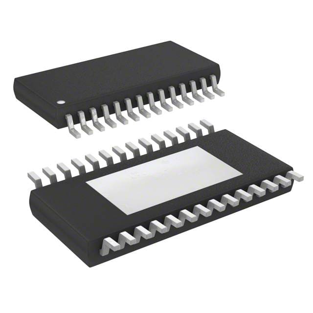
- Package: GUI/V+T
- Essence: Voltage Regulator
- Packaging/Quantity: Tape & Reel, 2500 units per reel
Specifications and Parameters
- Input Voltage Range: 2.7V to 5.5V
- Output Voltage Range: 0.8V to 3.6V
- Output Current: Up to 1A
- Quiescent Current: 17µA (typical)
- Operating Temperature Range: -40°C to +85°C
Pin Configuration
The MAX13325GUI/V+T has the following pin configuration:
- VIN: Input Voltage
- EN: Enable Control
- PGND: Power Ground
- SW: Switching Node
- FB: Feedback Voltage
- AGND: Analog Ground
- VOUT: Output Voltage
- BST: Boost Capacitor Connection
Functional Characteristics
- High Efficiency: The MAX13325GUI/V+T offers high efficiency power conversion, minimizing energy loss.
- Low Power Consumption: With a quiescent current of only 17µA, it ensures low power consumption during operation.
- Wide Input Voltage Range: It supports input voltages ranging from 2.7V to 5.5V, providing flexibility in various applications.
- Adjustable Output Voltage: The output voltage can be adjusted from 0.8V to 3.6V, allowing customization based on specific requirements.
Advantages and Disadvantages
Advantages: - High efficiency power conversion - Low power consumption - Wide input voltage range - Adjustable output voltage
Disadvantages: - Limited output current capacity (up to 1A)
Applicable Range of Products
The MAX13325GUI/V+T is suitable for a wide range of applications, including but not limited to: - Battery-powered devices - Portable electronics - IoT devices - Wearable devices
Working Principles
The MAX13325GUI/V+T is a voltage regulator that converts the input voltage to a regulated output voltage. It utilizes a switching topology to achieve high efficiency power conversion. The feedback voltage (FB) pin is used to control and stabilize the output voltage.
Detailed Application Field Plans
The MAX13325GUI/V+T can be applied in various fields, such as: 1. Mobile Devices: Provides efficient power management for smartphones and tablets. 2. Wireless Sensors: Enables reliable power supply for wireless sensor networks. 3. Medical Devices: Ensures stable power delivery for medical equipment. 4. Industrial Automation: Facilitates power management in industrial automation systems. 5. Automotive Electronics: Supports power regulation in automotive electronic systems.
Detailed Alternative Models
Some alternative models to the MAX13325GUI/V+T include: - MAX13326GUI/V+T - MAX13327GUI/V+T - MAX13328GUI/V+T - MAX13329GUI/V+T - MAX13330GUI/V+T
5 Common Technical Questions and Answers
Q: What is the maximum output current of the MAX13325GUI/V+T? A: The MAX13325GUI/V+T can provide an output current of up to 1A.
Q: What is the operating temperature range of the MAX13325GUI/V+T? A: The MAX13325GUI/V+T can operate within a temperature range of -40°C to +85°C.
Q: Can the output voltage be adjusted? A: Yes, the output voltage of the MAX13325GUI/V+T is adjustable from 0.8V to 3.6V.
Q: What is the typical quiescent current of the MAX13325GUI/V+T? A: The typical quiescent current of the MAX13325GUI/V+T is 17µA.
Q: What is the input voltage range supported by the MAX13325GUI/V+T? A: The MAX13325GUI/V+T can accept input voltages ranging from 2.7V to 5.5V.