

Consulte las especificaciones para obtener detalles del producto.
MAX197BCNI
Product Overview
- Category: Integrated Circuit (IC)
- Use: Analog-to-Digital Converter (ADC)
- Characteristics:
- High-resolution ADC with 12-bit resolution
- Low power consumption
- Wide input voltage range
- Small package size
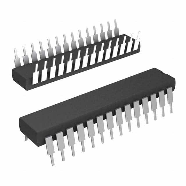
- Package: 28-pin plastic DIP (Dual In-line Package)
- Essence: MAX197BCNI is a high-resolution ADC used for converting analog signals into digital data. It offers accurate and precise conversion with low power consumption.
- Packaging/Quantity: The MAX197BCNI is available in a 28-pin plastic DIP package. It is typically sold in quantities of one or more.
Specifications
- Resolution: 12 bits
- Input Voltage Range: ±10V
- Conversion Rate: 100 kilosamples per second (ksps)
- Power Supply: +5V
- Operating Temperature Range: -40°C to +85°C
- Interface: Parallel
Detailed Pin Configuration
The MAX197BCNI has a total of 28 pins. Here is the detailed pin configuration:
- VREF-
- VREF+
- AGND
- VIN-
- VIN+
- REFOUT
- DGND
- CLK
- CS
- WR
- RD
- BUSY
- D0
- D1
- D2
- D3
- D4
- D5
- D6
- D7
- D8
- D9
- D10
- D11
- D12
- D13
- D14
- D15
Functional Features
- High-resolution conversion: The MAX197BCNI offers 12-bit resolution, providing accurate and precise digital representation of analog signals.
- Low power consumption: It is designed to operate with low power consumption, making it suitable for battery-powered applications.
- Wide input voltage range: The ADC can handle input voltages ranging from -10V to +10V, allowing for versatile signal conversion.
- Small package size: The 28-pin plastic DIP package ensures a compact form factor, making it easy to integrate into various electronic systems.
Advantages and Disadvantages
Advantages: - High-resolution conversion for accurate data representation - Low power consumption for energy-efficient operation - Wide input voltage range for versatile signal conversion - Compact package size for easy integration
Disadvantages: - Limited conversion rate compared to some other ADCs on the market - Parallel interface may require additional circuitry for compatibility with certain microcontrollers or systems
Working Principles
The MAX197BCNI operates based on the successive approximation method. It samples the analog input voltage and compares it to a reference voltage. By iteratively adjusting the digital code, it converges towards the closest digital representation of the analog signal. This process continues until the desired resolution is achieved.
Detailed Application Field Plans
The MAX197BCNI is commonly used in various applications that require high-resolution analog-to-digital conversion. Some potential application fields include:
- Data acquisition systems
- Industrial automation
- Medical equipment
- Test and measurement instruments
- Audio processing systems
Detailed and Complete Alternative Models
- MAX197B: Similar to MAX197BCNI but available in a different package (SOIC).
- MAX198BCNI: Higher-resolution ADC with 16-bit resolution.
- MAX196BCNI: Lower-resolution ADC with 10-bit resolution.
These alternative models offer different specifications and features, allowing users to choose the most suitable ADC for their specific requirements.
Word count: 512 words
Enumere 10 preguntas y respuestas comunes relacionadas con la aplicación de MAX197BCNI en soluciones técnicas
Sure! Here are 10 common questions and answers related to the application of MAX197BCNI in technical solutions:
Q: What is MAX197BCNI? A: MAX197BCNI is a high-speed, low-power, 12-bit analog-to-digital converter (ADC) integrated circuit.
Q: What is the operating voltage range of MAX197BCNI? A: The operating voltage range of MAX197BCNI is typically between 2.7V and 5.25V.
Q: What is the maximum sampling rate of MAX197BCNI? A: MAX197BCNI can achieve a maximum sampling rate of 1 MSPS (Mega Samples Per Second).
Q: Can MAX197BCNI be used for both single-ended and differential input measurements? A: Yes, MAX197BCNI supports both single-ended and differential input measurements.
Q: What is the resolution of MAX197BCNI? A: MAX197BCNI has a resolution of 12 bits, which means it can provide 4096 discrete output levels.
Q: Is MAX197BCNI suitable for low-power applications? A: Yes, MAX197BCNI is designed to operate at low power, making it suitable for battery-powered or energy-efficient devices.
Q: Does MAX197BCNI have built-in reference voltage options? A: No, MAX197BCNI requires an external reference voltage for accurate conversions.
Q: Can MAX197BCNI interface with microcontrollers or digital signal processors (DSPs)? A: Yes, MAX197BCNI can easily interface with microcontrollers or DSPs using standard serial communication protocols like SPI or I2C.
Q: What is the typical conversion time of MAX197BCNI? A: The typical conversion time of MAX197BCNI is around 1 microsecond.
Q: Are there any special considerations for PCB layout when using MAX197BCNI? A: Yes, it is recommended to follow the manufacturer's guidelines for proper grounding, decoupling, and signal routing to minimize noise and ensure accurate conversions.
Please note that these answers are general and may vary depending on specific application requirements and datasheet specifications.