

Consulte las especificaciones para obtener detalles del producto.
MAX5202ACUB+ - English Editing Encyclopedia Entry
Product Overview
Category
The MAX5202ACUB+ belongs to the category of integrated circuits (ICs).
Use
This IC is commonly used in electronic devices for digital-to-analog conversion.
Characteristics
- High precision and accuracy
- Low power consumption
- Wide operating voltage range
- Compact size
Package
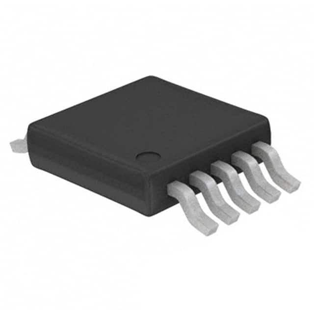
The MAX5202ACUB+ is available in a small outline integrated circuit (SOIC) package.
Essence
This IC serves as a key component in various electronic systems, enabling accurate conversion of digital signals into analog voltages.
Packaging/Quantity
The MAX5202ACUB+ is typically packaged in reels or tubes, with a quantity of 250 units per reel/tube.
Specifications
- Resolution: 12 bits
- Supply Voltage Range: 2.7V to 5.5V
- Operating Temperature Range: -40°C to +85°C
- Output Voltage Range: 0V to Vref
- Total Unadjusted Error: ±1 LSB (max)
- Power Consumption: 0.5mW (typ)
Detailed Pin Configuration
The MAX5202ACUB+ has a total of 16 pins, each serving a specific function. The pin configuration is as follows:
- VDD - Power supply input
- GND - Ground reference
- DIN - Digital input for data transfer
- CS - Chip select input
- SCLK - Serial clock input
- LDAC - Load DAC input
- REFOUT - Reference voltage output
- AGND - Analog ground reference
- OUTA - Analog output A
- OUTB - Analog output B
- OUTC - Analog output C
- OUTD - Analog output D
- REFIN - Reference voltage input
- REFSEL - Reference voltage selection input
- VREF - External reference voltage input
- NC - No connection
Functional Features
- High-resolution digital-to-analog conversion
- Serial interface for easy integration with microcontrollers
- Internal voltage reference for accurate output
- Power-down mode for reduced power consumption
- Output buffer amplifiers for driving external loads
Advantages and Disadvantages
Advantages
- High precision and accuracy in digital-to-analog conversion
- Wide operating voltage range allows compatibility with various systems
- Low power consumption for energy-efficient applications
- Compact size enables space-saving designs
Disadvantages
- Limited output voltage range may not be suitable for certain applications requiring higher voltages
- Lack of built-in protection features against overvoltage or short circuits
Working Principles
The MAX5202ACUB+ utilizes a digital-to-analog converter (DAC) to convert binary digital signals into corresponding analog voltages. It employs an internal voltage reference and output buffer amplifiers to ensure accurate and stable output. The IC can be controlled through a serial interface, allowing seamless integration with microcontrollers or other digital systems.
Detailed Application Field Plans
The MAX5202ACUB+ finds extensive application in various fields, including but not limited to: - Audio equipment - Industrial automation - Test and measurement instruments - Communication systems - Automotive electronics
Detailed and Complete Alternative Models
- MAX5204ACUB+
- MAX5206ACUB+
- MAX5208ACUB+
- MAX5210ACUB+
- MAX5212ACUB+
These alternative models offer similar functionality and characteristics, providing options for different resolution requirements and system specifications.
In conclusion, the MAX5202ACUB+ is a highly precise and efficient digital-to-analog converter integrated circuit. Its compact size, wide operating voltage range, and low power consumption make it suitable for various applications in different industries. However, designers should consider the limited output voltage range and absence of built-in protection features when selecting this IC for specific projects.
Enumere 10 preguntas y respuestas comunes relacionadas con la aplicación de MAX5202ACUB+ en soluciones técnicas
Sure! Here are 10 common questions and answers related to the application of MAX5202ACUB+ in technical solutions:
Q: What is the MAX5202ACUB+? A: The MAX5202ACUB+ is a high-precision, dual-channel, digital-to-analog converter (DAC) with a 16-bit resolution.
Q: What is the voltage range of the MAX5202ACUB+? A: The voltage range of the MAX5202ACUB+ is from -5V to +5V.
Q: How many channels does the MAX5202ACUB+ have? A: The MAX5202ACUB+ has two independent channels, allowing for simultaneous control of two analog outputs.
Q: What is the resolution of the MAX5202ACUB+? A: The MAX5202ACUB+ has a resolution of 16 bits, providing high precision in analog output generation.
Q: What is the interface used to communicate with the MAX5202ACUB+? A: The MAX5202ACUB+ uses a standard serial peripheral interface (SPI) for communication with microcontrollers or other devices.
Q: Can the MAX5202ACUB+ operate on a single power supply? A: Yes, the MAX5202ACUB+ can operate on a single power supply ranging from +2.7V to +5.25V.
Q: What is the typical settling time of the MAX5202ACUB+? A: The typical settling time of the MAX5202ACUB+ is 8µs, ensuring fast response in generating analog outputs.
Q: Does the MAX5202ACUB+ have internal reference voltages? A: No, the MAX5202ACUB+ requires external reference voltages for accurate analog output generation.
Q: Can the MAX5202ACUB+ be used in industrial applications? A: Yes, the MAX5202ACUB+ is suitable for various industrial applications requiring high-precision analog outputs.
Q: Are there any evaluation boards or development kits available for the MAX5202ACUB+? A: Yes, Maxim Integrated provides evaluation kits and software tools to facilitate the development and testing of applications using the MAX5202ACUB+.