

Consulte las especificaciones para obtener detalles del producto.
MAX5302CUA+T
Product Overview
- Category: Integrated Circuit (IC)
- Use: Digital-to-Analog Converter (DAC)
- Characteristics: High-resolution, low-power consumption
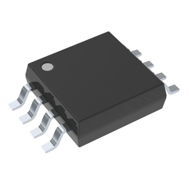
- Package: 8-pin µMAX® package
- Essence: Converts digital signals into analog voltages
- Packaging/Quantity: Tape and reel packaging, quantity varies
Specifications
- Resolution: 12 bits
- Supply Voltage: 2.7V to 5.5V
- Operating Temperature Range: -40°C to +85°C
- Output Voltage Range: 0V to VREF
- Output Current: ±1mA
- Power Consumption: 0.5mW (typical)
Pin Configuration
The MAX5302CUA+T has the following pin configuration:
```
| | --|VDD VOUT|-- --|GND AGND|-- --|SDI SCLK|-- --|LDAC CS |-- |___________| ```
- VDD: Positive power supply
- GND: Ground reference
- SDI: Serial data input
- SCLK: Serial clock input
- LDAC: Load DAC input
- CS: Chip select input
- AGND: Analog ground
- VOUT: Analog output voltage
Functional Features
- High-resolution DAC with 12-bit resolution
- Low-power consumption for energy-efficient applications
- Serial interface for easy integration with microcontrollers
- Internal reference voltage for simplified design
- Fast settling time for accurate and responsive analog outputs
Advantages and Disadvantages
Advantages: - High resolution allows for precise analog voltage generation - Low power consumption extends battery life in portable devices - Serial interface simplifies communication with microcontrollers - Fast settling time ensures quick response to input changes
Disadvantages: - Limited output current may not be suitable for high-power applications - Restricted operating temperature range may limit certain industrial uses
Working Principles
The MAX5302CUA+T is a digital-to-analog converter (DAC) that converts digital signals into analog voltages. It utilizes a 12-bit resolution to provide high precision in generating analog outputs. The DAC operates with a supply voltage ranging from 2.7V to 5.5V and consumes low power, making it suitable for battery-powered devices.
The device features a serial interface, allowing easy integration with microcontrollers. It accepts serial data input (SDI) and clock input (SCLK) to receive digital signals. The load DAC input (LDAC) and chip select input (CS) control the loading and selection of the DAC output. The analog output voltage (VOUT) can be adjusted within the range of 0V to the reference voltage (VREF).
Detailed Application Field Plans
The MAX5302CUA+T finds applications in various fields, including:
- Audio Systems: Used in audio equipment to convert digital audio signals into analog voltages for amplification and playback.
- Instrumentation: Employed in test and measurement instruments to generate precise analog signals for calibration and signal generation.
- Industrial Control: Integrated into industrial control systems to provide accurate analog control signals for process control and automation.
- Communication Systems: Utilized in communication devices to convert digital signals into analog voltages for modulation and transmission.
- Automotive Electronics: Incorporated in automotive systems for functions such as audio processing, sensor calibration, and control signal generation.
Detailed and Complete Alternative Models
- MAX5312CUA+T: Similar to MAX5302CUA+T but with a higher resolution of 16 bits.
- MAX5322CUA+T: Offers similar functionality with a 10-bit resolution and lower power consumption.
- MAX5382CUA+T: Provides a higher output current of ±2mA while maintaining a 12-bit resolution.
These alternative models offer different specifications and features, allowing users to choose the most suitable DAC for their specific requirements.
Word count: 511 words
Enumere 10 preguntas y respuestas comunes relacionadas con la aplicación de MAX5302CUA+T en soluciones técnicas
Sure! Here are 10 common questions and answers related to the application of MAX5302CUA+T in technical solutions:
Q: What is the MAX5302CUA+T? A: The MAX5302CUA+T is a digital-to-analog converter (DAC) IC that converts digital signals into analog voltages.
Q: What is the voltage range supported by MAX5302CUA+T? A: The MAX5302CUA+T supports a voltage range of 0V to VREF, where VREF is the reference voltage provided externally.
Q: What is the resolution of MAX5302CUA+T? A: The MAX5302CUA+T has a resolution of 12 bits, allowing for precise control over the analog output.
Q: How can I interface with the MAX5302CUA+T? A: The MAX5302CUA+T can be interfaced using a serial peripheral interface (SPI) or a parallel interface.
Q: Can I use the MAX5302CUA+T in battery-powered applications? A: Yes, the MAX5302CUA+T has low power consumption and can be used in battery-powered applications.
Q: What is the maximum sampling rate of the MAX5302CUA+T? A: The MAX5302CUA+T has a maximum sampling rate of 1 MSPS (Mega Samples Per Second).
Q: Does the MAX5302CUA+T have built-in voltage references? A: No, the MAX5302CUA+T requires an external voltage reference for accurate conversion.
Q: Can I use the MAX5302CUA+T in industrial applications? A: Yes, the MAX5302CUA+T is suitable for industrial applications due to its wide temperature range and robustness.
Q: What is the output voltage settling time of the MAX5302CUA+T? A: The MAX5302CUA+T has a typical output voltage settling time of 10 µs.
Q: Are there any evaluation boards or development kits available for the MAX5302CUA+T? A: Yes, Maxim Integrated provides evaluation boards and development kits for easy prototyping and testing of the MAX5302CUA+T.
Please note that these answers are general and may vary depending on specific application requirements. It's always recommended to refer to the datasheet and application notes provided by the manufacturer for detailed information.