

Consulte las especificaciones para obtener detalles del producto.
MAX5661GCB+ - English Editing Encyclopedia Entry
Product Overview
Category
MAX5661GCB+ belongs to the category of integrated circuits (ICs).
Use
This product is commonly used in electronic devices for analog-to-digital conversion.
Characteristics
- High precision and accuracy
- Low power consumption
- Wide operating voltage range
- Compact package size
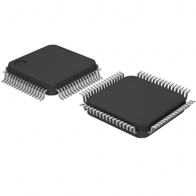
Package
MAX5661GCB+ is available in a small form factor package, which ensures easy integration into various electronic systems.
Essence
The essence of MAX5661GCB+ lies in its ability to convert analog signals into digital data with high precision and reliability.
Packaging/Quantity
This product is typically packaged in reels or trays, with a quantity of 250 units per reel/tray.
Specifications
- Resolution: 16 bits
- Input Voltage Range: 0V to VREF
- Supply Voltage Range: 2.7V to 5.5V
- Operating Temperature Range: -40°C to +85°C
- Conversion Rate: Up to 500 kSPS (Samples Per Second)
- Interface: Serial Peripheral Interface (SPI)
Detailed Pin Configuration
The pin configuration of MAX5661GCB+ is as follows:
| Pin Number | Pin Name | Description | |------------|----------|-------------| | 1 | VDD | Power supply voltage | | 2 | GND | Ground reference | | 3 | DIN | Serial data input | | 4 | SCLK | Serial clock input | | 5 | CS | Chip select input | | 6 | DOUT | Serial data output | | 7 | REF | Reference voltage input | | 8 | AGND | Analog ground reference |
Functional Features
- High-resolution analog-to-digital conversion
- Programmable reference voltage
- Low power consumption
- SPI interface for easy integration with microcontrollers
Advantages and Disadvantages
Advantages
- High precision and accuracy in analog-to-digital conversion
- Wide operating voltage range allows for versatile applications
- Compact package size enables integration into space-constrained designs
- Low power consumption prolongs battery life in portable devices
Disadvantages
- Limited conversion rate compared to some other models in the market
- Requires an external reference voltage source
Working Principles
MAX5661GCB+ utilizes a successive approximation register (SAR) architecture for analog-to-digital conversion. The input analog signal is compared against a reference voltage, and the digital output is generated based on the comparison results.
Detailed Application Field Plans
MAX5661GCB+ finds applications in various fields, including but not limited to: - Industrial automation - Medical equipment - Test and measurement instruments - Audio processing systems - Data acquisition systems
Detailed and Complete Alternative Models
Some alternative models that offer similar functionality to MAX5661GCB+ are: - AD7685 from Analog Devices - MCP3421 from Microchip Technology - LTC1867 from Linear Technology - ADS1115 from Texas Instruments
These alternative models provide options for different resolution, speed, and interface requirements.
In conclusion, MAX5661GCB+ is a high-precision analog-to-digital converter IC with a compact form factor and low power consumption. It offers reliable performance and finds applications in various industries.
Enumere 10 preguntas y respuestas comunes relacionadas con la aplicación de MAX5661GCB+ en soluciones técnicas
Sure! Here are 10 common questions and answers related to the application of MAX5661GCB+ in technical solutions:
Q1: What is MAX5661GCB+? A1: MAX5661GCB+ is a high-performance, low-power, 16-bit digital-to-analog converter (DAC) that can be used in various technical applications.
Q2: What is the voltage range of MAX5661GCB+? A2: The voltage range of MAX5661GCB+ is typically ±10V, which can be adjusted using external references.
Q3: What is the resolution of MAX5661GCB+? A3: MAX5661GCB+ has a resolution of 16 bits, allowing for precise analog output control.
Q4: How many channels does MAX5661GCB+ have? A4: MAX5661GCB+ has four independent DAC channels, each capable of generating an analog output.
Q5: What is the maximum update rate of MAX5661GCB+? A5: The maximum update rate of MAX5661GCB+ is typically 500 kSPS (thousand samples per second).
Q6: Can MAX5661GCB+ operate with a single power supply? A6: Yes, MAX5661GCB+ can operate with a single power supply, typically ranging from +2.7V to +5.25V.
Q7: Is MAX5661GCB+ compatible with SPI interface? A7: Yes, MAX5661GCB+ supports a serial peripheral interface (SPI) for easy integration into microcontroller-based systems.
Q8: Does MAX5661GCB+ have built-in reference voltage? A8: No, MAX5661GCB+ requires an external reference voltage for accurate analog output generation.
Q9: Can MAX5661GCB+ be used in industrial applications? A9: Yes, MAX5661GCB+ is suitable for various industrial applications, including process control and automation.
Q10: What is the package type of MAX5661GCB+? A10: MAX5661GCB+ is available in a 24-pin TQFN (Thin Quad Flat No-Lead) package, which is compact and easy to solder.
Please note that these answers are general and may vary depending on the specific requirements and use cases.