

Consulte las especificaciones para obtener detalles del producto.
MAX6846KASD3+T
Product Overview
- Category: Integrated Circuit (IC)
- Use: Power Management
- Characteristics: High Efficiency, Low Power Consumption
- Package: Surface Mount
- Essence: Voltage Regulator
- Packaging/Quantity: Tape and Reel, 3000 units per reel
Specifications
- Input Voltage Range: 2.7V to 5.5V
- Output Voltage Range: 1.2V to 3.3V
- Output Current: Up to 500mA
- Quiescent Current: 20µA (typical)
- Operating Temperature Range: -40°C to +85°C
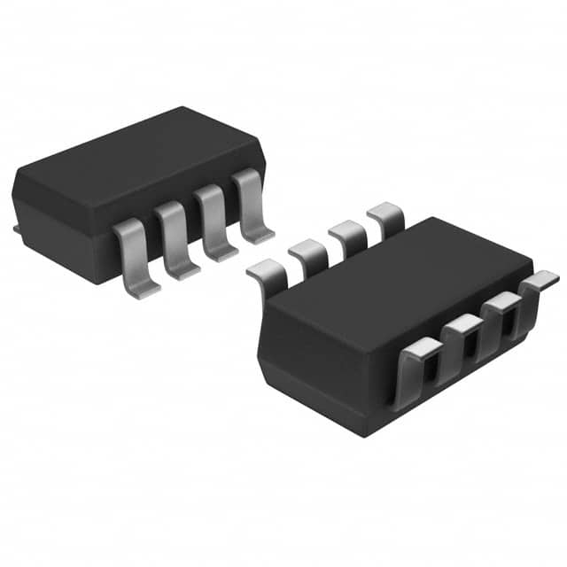
Detailed Pin Configuration
The MAX6846KASD3+T has a total of 6 pins:
- VIN: Input voltage pin
- GND: Ground pin
- EN: Enable pin
- FB: Feedback pin
- VOUT: Output voltage pin
- PG: Power Good pin
Functional Features
- High Efficiency: The MAX6846KASD3+T offers high efficiency power conversion, minimizing energy loss.
- Low Power Consumption: With a quiescent current of only 20µA, it ensures minimal power consumption during standby or idle modes.
- Power Good Indicator: The PG pin provides a signal indicating when the output voltage is within the specified range.
- Enable Control: The EN pin allows for easy on/off control of the voltage regulator.
Advantages and Disadvantages
Advantages: - High efficiency power conversion - Low power consumption - Power good indicator for voltage monitoring - Easy enable/disable control
Disadvantages: - Limited output current capacity (up to 500mA)
Working Principles
The MAX6846KASD3+T is a voltage regulator IC that takes an input voltage within the range of 2.7V to 5.5V and provides a regulated output voltage between 1.2V and 3.3V. It achieves this by using internal circuitry to step down the input voltage to the desired output voltage level.
The EN pin allows for easy control of the regulator's operation. When the EN pin is high, the regulator is enabled and actively regulates the output voltage. Conversely, when the EN pin is low, the regulator enters a low-power standby mode, reducing power consumption.
The FB pin is used for feedback control, ensuring the output voltage remains stable and within the specified range. The PG pin provides a signal indicating whether the output voltage is within the desired range, allowing for voltage monitoring.
Detailed Application Field Plans
The MAX6846KASD3+T is commonly used in various applications where efficient power management is required. Some potential application fields include:
- Portable Electronics: It can be used in smartphones, tablets, and other battery-powered devices to regulate the voltage supplied to different components.
- IoT Devices: The IC can be utilized in Internet of Things (IoT) devices, such as sensors and smart home devices, to efficiently manage power consumption.
- Industrial Automation: It finds applications in industrial automation systems, providing stable and regulated power to control units and sensors.
- Automotive Electronics: The voltage regulator can be employed in automotive electronics, ensuring reliable power supply to various components.
Detailed and Complete Alternative Models
- LM1117-3.3: A popular alternative with similar specifications and functionality.
- LT1763-3.3: Another alternative offering high efficiency and low dropout voltage.
- TPS79633: An alternative model known for its low noise and high PSRR (Power Supply Rejection Ratio).
These alternative models provide similar voltage regulation capabilities and can be considered as substitutes for the MAX6846KASD3+T in various applications.
Word count: 496 words
Enumere 10 preguntas y respuestas comunes relacionadas con la aplicación de MAX6846KASD3+T en soluciones técnicas
Sure! Here are 10 common questions and answers related to the application of MAX6846KASD3+T in technical solutions:
Q: What is the MAX6846KASD3+T? A: The MAX6846KASD3+T is a voltage monitor and reset IC designed for use in various technical solutions.
Q: What is the purpose of the MAX6846KASD3+T? A: The purpose of this IC is to monitor the voltage level of a system and generate a reset signal when the voltage falls below a specified threshold.
Q: What voltage range does the MAX6846KASD3+T support? A: The MAX6846KASD3+T supports a voltage range from 1.6V to 5.5V.
Q: How does the MAX6846KASD3+T generate a reset signal? A: It generates a reset signal by pulling the RESET output pin low when the monitored voltage falls below the specified threshold.
Q: Can I adjust the voltage threshold for generating a reset signal? A: Yes, the voltage threshold can be adjusted using external resistors connected to the VTH pin.
Q: What is the typical reset time delay of the MAX6846KASD3+T? A: The typical reset time delay is around 200ms.
Q: Does the MAX6846KASD3+T have any built-in hysteresis? A: Yes, it has a built-in hysteresis of approximately 100mV to prevent false triggering due to voltage fluctuations.
Q: Can the MAX6846KASD3+T be used in battery-powered applications? A: Yes, it can be used in battery-powered applications as it operates within a wide voltage range and has low quiescent current.
Q: What is the package type of the MAX6846KASD3+T? A: The MAX6846KASD3+T is available in a small 8-pin SOT23 package.
Q: Are there any application notes or reference designs available for the MAX6846KASD3+T? A: Yes, Maxim Integrated provides application notes and reference designs on their website to help users implement the MAX6846KASD3+T in various technical solutions.
Please note that these answers are general and may vary depending on the specific requirements and use cases. It's always recommended to refer to the datasheet and documentation provided by the manufacturer for accurate information.