

Consulte las especificaciones para obtener detalles del producto.
AT17LV010A-10JC
Product Overview
Category
AT17LV010A-10JC belongs to the category of programmable logic devices (PLDs).
Use
This product is commonly used in digital circuit design and implementation. It provides a flexible and customizable solution for various applications.
Characteristics
- Programmable: The AT17LV010A-10JC can be programmed to perform specific functions based on user requirements.
- High-speed operation: It operates at a speed of 10 nanoseconds, allowing for efficient data processing.
- Low power consumption: This device is designed to minimize power usage, making it suitable for battery-powered applications.
- Non-volatile memory: The programmed configuration remains intact even when power is removed.
Package
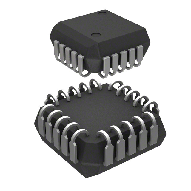
The AT17LV010A-10JC is available in a 32-pin PLCC (Plastic Leaded Chip Carrier) package.
Essence
The essence of this product lies in its ability to provide reconfigurable logic functionality, enabling designers to implement complex digital circuits with ease.
Packaging/Quantity
The AT17LV010A-10JC is typically packaged in reels or tubes, with a quantity of 100 units per package.
Specifications
- Operating Voltage: 3.3V
- Maximum Operating Frequency: 100 MHz
- Number of Logic Cells: 1,000
- Memory Capacity: 128 kilobits
- I/O Pins: 24
- Temperature Range: -40°C to +85°C
Detailed Pin Configuration
The AT17LV010A-10JC has a total of 32 pins. The pin configuration is as follows:
- VCCIO
- GND
- CE#
- OE#
- WE#
- A0
- A1
- A2
- A3
- A4
- A5
- A6
- A7
- A8
- A9
- A10
- A11
- NC
- I/O0
- I/O1
- I/O2
- I/O3
- I/O4
- I/O5
- I/O6
- I/O7
- I/O8
- I/O9
- I/O10
- I/O11
- GND
- VCC
Functional Features
- In-system programmability: The AT17LV010A-10JC can be programmed while in the target system, allowing for easy updates and modifications.
- JTAG interface: It supports Joint Test Action Group (JTAG) boundary scan testing, enabling efficient debugging and testing of the device.
- Security features: This PLD offers security bit options to protect the programmed configuration from unauthorized access or copying.
Advantages and Disadvantages
Advantages
- Flexibility: The reprogrammable nature of this device allows for quick prototyping and design iterations.
- Cost-effective: By using a single programmable device, designers can reduce the need for multiple discrete components.
- Low power consumption: The AT17LV010A-10JC is designed to operate efficiently with minimal power requirements.
Disadvantages
- Limited capacity: With a memory capacity of 128 kilobits, this PLD may not be suitable for applications requiring larger logic designs.
- Programming complexity: Programming the device requires specialized knowledge and tools, which may pose a challenge for inexperienced users.
Working Principles
The AT17LV010A-10JC utilizes a combination of programmable logic cells and non-volatile memory elements to implement user-defined logic functions. These logic cells can be interconnected and configured through programming to create the desired digital circuit.
Detailed Application Field Plans
The AT17LV010A-10JC finds applications in various fields, including:
- Embedded Systems: It can be used to implement custom logic functions in microcontroller-based systems.
- Communication Systems: This PLD can be employed in networking equipment for protocol handling and data processing.
- Industrial Automation: It enables the implementation of control and monitoring functions in industrial automation systems.
- Automotive Electronics: The AT17LV010A-10JC can be utilized in automotive electronics for tasks such as sensor interfacing and control logic.
Detailed and Complete Alternative Models
- AT17LV010A-15JC: Similar to the AT17LV010A-10JC, but operates at a speed of 15 nanoseconds.
- AT17LV010A-20JC: Similar to the AT17LV010A-10JC, but operates at a speed of 20 nanoseconds.
- AT17LV020A-10JC: A higher-capacity alternative with 256 kilobits of memory.
These alternative models provide options based on
Enumere 10 preguntas y respuestas comunes relacionadas con la aplicación de AT17LV010A-10JC en soluciones técnicas
Sure! Here are 10 common questions and answers related to the application of AT17LV010A-10JC in technical solutions:
Q: What is the AT17LV010A-10JC? A: The AT17LV010A-10JC is a low-voltage, high-performance, one-time programmable (OTP) field-programmable gate array (FPGA) device.
Q: What are the key features of the AT17LV010A-10JC? A: Some key features include a 1Mb density, 10ns access time, 3.3V operation, and JTAG boundary-scan support.
Q: How can I program the AT17LV010A-10JC? A: The AT17LV010A-10JC can be programmed using industry-standard programming tools such as the Atmel ISP software or third-party programmers.
Q: What are some typical applications for the AT17LV010A-10JC? A: The AT17LV010A-10JC is commonly used in applications such as telecommunications, networking, industrial control systems, and automotive electronics.
Q: Can the AT17LV010A-10JC be reprogrammed after it has been programmed once? A: No, the AT17LV010A-10JC is a one-time programmable device, meaning that it cannot be reprogrammed once it has been programmed.
Q: What is the power supply voltage range for the AT17LV010A-10JC? A: The AT17LV010A-10JC operates at a voltage range of 3.0V to 3.6V.
Q: Does the AT17LV010A-10JC support JTAG boundary-scan testing? A: Yes, the AT17LV010A-10JC supports JTAG boundary-scan testing, which allows for efficient testing and debugging of the device.
Q: What is the maximum operating frequency of the AT17LV010A-10JC? A: The AT17LV010A-10JC has a maximum operating frequency of 100MHz.
Q: Can I use the AT17LV010A-10JC in a high-temperature environment? A: Yes, the AT17LV010A-10JC is designed to operate in a wide temperature range, typically from -40°C to +85°C.
Q: Are there any specific design considerations when using the AT17LV010A-10JC? A: Some design considerations include proper decoupling capacitor placement, signal integrity management, and adherence to recommended power supply and ground routing guidelines.
Please note that these answers are general and may vary depending on the specific requirements and application of the AT17LV010A-10JC in your technical solution.