

Consulte las especificaciones para obtener detalles del producto.
PIC18F2550-I/SO
Product Overview
Category
The PIC18F2550-I/SO belongs to the category of microcontrollers.
Use
This microcontroller is commonly used in various electronic applications that require embedded control and processing capabilities.
Characteristics
- High-performance 8-bit RISC architecture
- Flash program memory with self-read/write capability
- USB 2.0 Full-Speed compatible
- Low power consumption
- Wide operating voltage range
- Multiple communication interfaces (UART, SPI, I2C)
- Analog-to-Digital Converter (ADC) module
- Enhanced Capture/Compare/PWM (ECCP) module
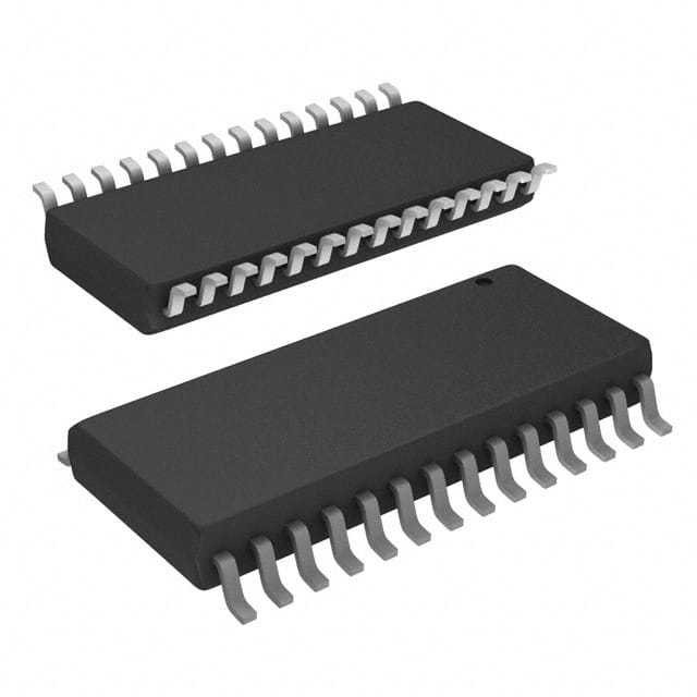
Package
The PIC18F2550-I/SO is available in a small outline (SO) package.
Essence
The essence of the PIC18F2550-I/SO lies in its ability to provide efficient and reliable control and processing capabilities for various electronic applications.
Packaging/Quantity
This microcontroller is typically packaged in reels or tubes, with a quantity of 250 units per reel/tube.
Specifications
- Microcontroller Family: PIC18F
- CPU Speed: Up to 48 MHz
- Program Memory Size: 32 KB
- RAM Size: 2 KB
- Number of I/O Pins: 24
- Operating Voltage Range: 2.0V to 5.5V
- Communication Interfaces: UART, SPI, I2C
- ADC Resolution: 10-bit
- ECCP Channels: 2
- USB Version: 2.0 Full-Speed
Detailed Pin Configuration
The PIC18F2550-I/SO has a total of 28 pins, each serving a specific purpose. The pin configuration is as follows:
- VDD - Power supply voltage
- VSS - Ground
- RA0 - General-purpose I/O pin
- RA1 - General-purpose I/O pin
- RA2 - General-purpose I/O pin
- RA3 - General-purpose I/O pin
- RA4 - General-purpose I/O pin
- RA5 - General-purpose I/O pin
- MCLR - Master Clear (Reset) input
- VUSB - USB power supply voltage
- RB0/INT0 - General-purpose I/O pin / External Interrupt 0
- RB1/INT1 - General-purpose I/O pin / External Interrupt 1
- RB2/INT2 - General-purpose I/O pin / External Interrupt 2
- RB3/INT3 - General-purpose I/O pin / External Interrupt 3
- RB4/KBI0/PGM - General-purpose I/O pin / Keyboard Interrupt 0 / In-Circuit Serial Programming
- RB5/KBI1/PGC - General-purpose I/O pin / Keyboard Interrupt 1 / ICSP Clock
- RB6/KBI2/PGD - General-purpose I/O pin / Keyboard Interrupt 2 / ICSP Data
- RB7/KBI3/PGM - General-purpose I/O pin / Keyboard Interrupt 3 / In-Circuit Serial Programming
- VPP - Programming voltage input
- OSC1/CLKI - Oscillator input
- OSC2/CLKO - Oscillator output
- RC0/T1OSO/T13CKI - General-purpose I/O pin / Timer1 Oscillator Output / Timer1 External Clock Input
- RC1/T1OSI/CCP2 - General-purpose I/O pin / Timer1 Oscillator Input / CCP2
- RC2/CCP1 - General-purpose I/O pin / CCP1
Functional Features
The PIC18F2550-I/SO offers several functional features that enhance its usability and performance:
- High-performance RISC architecture: The microcontroller's RISC architecture allows for efficient execution of instructions, resulting in faster processing speeds.
- Flash program memory: The self-read/write capability of the flash program memory enables easy and convenient programming of the microcontroller.
- USB 2.0 Full-Speed compatibility: The microcontroller supports USB 2.0 Full-Speed communication, making it suitable for applications requiring USB connectivity.
- Low power consumption: The microcontroller is designed to operate with low power consumption, making it ideal for battery-powered devices.
- Multiple communication interfaces: The presence of UART, SPI, and I2C interfaces allows for seamless integration with various peripheral devices.
- Analog-to-Digital Converter (ADC) module: The built-in ADC module enables the microcontroller to convert analog signals into digital values, expanding its range of applications.
- Enhanced Capture/Compare/PWM (ECCP) module: The ECCP module provides advanced control capabilities, allowing precise timing and control of external devices.
Advantages and Disadvantages
#
Enumere 10 preguntas y respuestas comunes relacionadas con la aplicación de PIC18F2550-I/SO en soluciones técnicas
What is the maximum operating frequency of PIC18F2550-I/SO?
- The maximum operating frequency of PIC18F2550-I/SO is 48 MHz.
What are the key features of PIC18F2550-I/SO?
- The key features of PIC18F2550-I/SO include USB 2.0, 13 channels of 10-bit Analog-to-Digital (A/D) converter, and up to 28 KB of flash program memory.
Can PIC18F2550-I/SO be used for USB applications?
- Yes, PIC18F2550-I/SO is specifically designed for USB applications and supports full-speed USB operation.
What programming language can be used to program PIC18F2550-I/SO?
- PIC18F2550-I/SO can be programmed using languages such as C, Assembly, and other high-level languages supported by Microchip's MPLAB® XC compilers.
Does PIC18F2550-I/SO have built-in communication interfaces?
- Yes, PIC18F2550-I/SO features built-in communication interfaces including USART, SPI, and I2C.
What are the power supply requirements for PIC18F2550-I/SO?
- PIC18F2550-I/SO operates with a voltage range of 2.0V to 5.5V, making it suitable for various power supply configurations.
Is PIC18F2550-I/SO suitable for low-power applications?
- Yes, PIC18F2550-I/SO offers low-power modes and features that make it suitable for low-power applications.
Can PIC18F2550-I/SO be used in industrial control systems?
- Yes, PIC18F2550-I/SO is suitable for industrial control systems due to its robust features and capabilities.
Are there development tools available for PIC18F2550-I/SO?
- Yes, Microchip provides a range of development tools and software support for PIC18F2550-I/SO, including MPLAB X IDE and various programmers/debuggers.
What are the typical applications of PIC18F2550-I/SO?
- Typical applications of PIC18F2550-I/SO include USB-based embedded systems, consumer electronics, industrial automation, and more.