

Consulte las especificaciones para obtener detalles del producto.
TC4423AVOE713
Basic Information Overview
- Category: Integrated Circuit (IC)
- Use: Driver for MOSFETs and IGBTs
- Characteristics:
- High peak output current
- Wide input voltage range
- Fast rise and fall times
- Low propagation delay
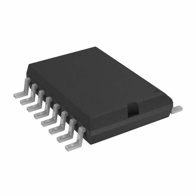
- Package: SOIC-8
- Essence: Power MOSFET and IGBT driver
- Packaging/Quantity: Tape and Reel, 2500 units per reel
Specifications
- Supply Voltage: 4.5V to 18V
- Output Current: 9A (peak), 2A (continuous)
- Input Threshold Voltage: 2.5V (typical)
- Rise/Fall Time: 25ns (typical)
- Propagation Delay: 55ns (typical)
- Operating Temperature Range: -40°C to +125°C
Detailed Pin Configuration
- VDD: Positive supply voltage
- IN: Input control signal
- LO: Low-side gate driver output
- HO: High-side gate driver output
- VB: Bootstrap supply voltage
- HB: Bootstrap high-side gate drive return
- LB: Bootstrap low-side gate drive return
- GND: Ground reference
Functional Features
- High peak output current allows driving power MOSFETs and IGBTs efficiently.
- Wide input voltage range enables compatibility with various control circuits.
- Fast rise and fall times minimize switching losses and improve overall system efficiency.
- Low propagation delay ensures accurate and synchronized switching of the power devices.
Advantages
- Robust and reliable performance in demanding applications.
- Compact SOIC-8 package offers space-saving benefits.
- Suitable for both high-side and low-side drive applications.
- Provides efficient and precise control over power MOSFETs and IGBTs.
Disadvantages
- Limited output current compared to some specialized drivers.
- Requires external bootstrap components for high-side drive operation.
- Not suitable for driving other types of devices such as BJTs or diodes.
Working Principles
The TC4423AVOE713 is a high-speed driver IC designed to control the switching of power MOSFETs and IGBTs. It operates by receiving an input control signal (IN) and generating corresponding gate drive signals (LO and HO) for the low-side and high-side power devices, respectively. The bootstrap supply voltage (VB) is used to provide the necessary gate drive voltage for the high-side device. By controlling the timing and duration of the gate drive signals, the TC4423AVOE713 ensures efficient and synchronized switching of the power devices.
Detailed Application Field Plans
The TC4423AVOE713 is widely used in various applications that require precise and efficient control of power MOSFETs and IGBTs. Some common application fields include: - Motor control systems - Switching power supplies - DC-DC converters - Inverters - LED lighting systems - Automotive electronics
Detailed and Complete Alternative Models
- TC4420CPA: 6A Dual MOSFET Driver, DIP-8 package
- TC4424EOA: 9A High-Speed MOSFET Driver, SOIC-8 package
- TC4452VPA: 12A Dual MOSFET Driver, PDIP-8 package
- TC4427EOA: 1.5A Dual MOSFET Driver, SOIC-8 package
- TC4429CPA: 6A Dual MOSFET Driver, DIP-8 package
(Note: This list is not exhaustive and there may be other alternative models available in the market.)
Word count: 409 words
Enumere 10 preguntas y respuestas comunes relacionadas con la aplicación de TC4423AVOE713 en soluciones técnicas
Sure! Here are 10 common questions and answers related to the application of TC4423AVOE713 in technical solutions:
Q: What is TC4423AVOE713? A: TC4423AVOE713 is a high-speed, dual MOSFET driver IC used for driving N-channel MOSFETs in various applications.
Q: What is the maximum voltage rating of TC4423AVOE713? A: The maximum voltage rating of TC4423AVOE713 is typically around 18V.
Q: Can TC4423AVOE713 be used to drive other types of transistors besides MOSFETs? A: No, TC4423AVOE713 is specifically designed for driving N-channel MOSFETs.
Q: What is the maximum output current capability of TC4423AVOE713? A: TC4423AVOE713 can typically provide up to 9A of peak output current.
Q: Is TC4423AVOE713 compatible with both 3.3V and 5V logic levels? A: Yes, TC4423AVOE713 is compatible with both 3.3V and 5V logic levels, making it versatile for different microcontroller or FPGA interfaces.
Q: Does TC4423AVOE713 have built-in protection features? A: Yes, TC4423AVOE713 has built-in undervoltage lockout (UVLO) and thermal shutdown protection to ensure safe operation.
Q: Can TC4423AVOE713 handle PWM signals? A: Yes, TC4423AVOE713 can handle PWM signals with its fast rise and fall times, making it suitable for motor control and power conversion applications.
Q: What is the operating temperature range of TC4423AVOE713? A: The operating temperature range of TC4423AVOE713 is typically between -40°C to 125°C.
Q: Can TC4423AVOE713 be used in high-frequency switching applications? A: Yes, TC4423AVOE713 has a high-speed switching capability, making it suitable for high-frequency applications such as switch-mode power supplies.
Q: Is there a recommended layout or PCB design guideline for using TC4423AVOE713? A: Yes, the datasheet of TC4423AVOE713 provides recommended layout and PCB design guidelines to ensure optimal performance and minimize noise coupling.
Please note that the answers provided here are general and may vary depending on specific application requirements. It is always recommended to refer to the datasheet and consult with the manufacturer for detailed information and application-specific considerations.