

Consulte las especificaciones para obtener detalles del producto.
N25Q512A81GSF40G
Basic Information Overview
- Category: Non-volatile Memory
- Use: Data storage and retrieval
- Characteristics:
- High capacity
- Fast read/write speeds
- Low power consumption
- Reliable performance
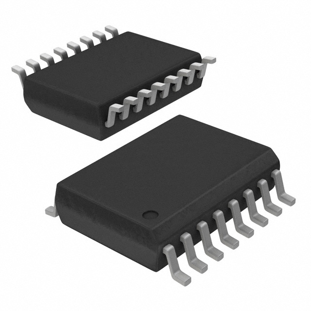
- Package: SOP (Small Outline Package)
- Essence: Flash memory chip
- Packaging/Quantity: Individually packaged, quantity varies based on order size
Specifications
- Capacity: 512 Megabits (64 Megabytes)
- Interface: Serial Peripheral Interface (SPI)
- Operating Voltage: 2.7V - 3.6V
- Operating Temperature Range: -40°C to +85°C
- Erase/Program Cycles: 100,000 cycles (minimum)
- Data Retention: 20 years (minimum)
Detailed Pin Configuration
The N25Q512A81GSF40G has a total of 8 pins. The pin configuration is as follows:
- Chip Select (/CS) - Active low input used to enable/disable the chip
- Serial Clock (SCK) - Input for synchronizing data transfer
- Serial Data Input (SI) - Input for sending data to the chip
- Serial Data Output (SO) - Output for receiving data from the chip
- Hold (/HOLD) - Input used to pause ongoing operations
- Write Protect (/WP) - Input used to protect the memory from being written
- Ground (GND) - Reference ground connection
- Power Supply (VCC) - Power supply input
Functional Features
- High-speed data transfer with SPI interface
- Efficient erase and programming operations
- Sector-based architecture for flexible data management
- Advanced security features for data protection
- Software and hardware write protection options
- Support for multiple operating modes
Advantages
- Large storage capacity for data-intensive applications
- Fast read/write speeds enable quick data access
- Low power consumption prolongs battery life in portable devices
- Reliable performance ensures data integrity
- Flexible sector-based architecture allows efficient data management
Disadvantages
- Limited erase/program cycles may affect longevity in certain applications
- Higher cost compared to traditional non-volatile memory options
- Requires additional circuitry for proper interfacing
Working Principles
The N25Q512A81GSF40G is based on the NAND flash memory technology. It utilizes a series of floating-gate transistors to store and retrieve digital data. The memory cells are organized into sectors, allowing for efficient read, write, and erase operations. The SPI interface facilitates communication between the chip and the host device, enabling seamless data transfer.
Detailed Application Field Plans
The N25Q512A81GSF40G is widely used in various applications, including: 1. Solid-state drives (SSDs) 2. Embedded systems 3. Networking equipment 4. Automotive electronics 5. Industrial control systems
Detailed and Complete Alternative Models
- N25Q256A13EF840E - 256 Megabit (32 Megabyte) capacity, same package and interface
- N25Q1T16A13EF840E - 1 Terabit (128 Gigabyte) capacity, same package and interface
- MX25L51245GZNI-10G - 512 Megabit (64 Megabyte) capacity, different package and interface
These alternative models offer similar functionality and can be considered as replacements for the N25Q512A81GSF40G based on specific requirements.
Word count: 446 words
Enumere 10 preguntas y respuestas comunes relacionadas con la aplicación de N25Q512A81GSF40G en soluciones técnicas
Sure! Here are 10 common questions and answers related to the application of N25Q512A81GSF40G in technical solutions:
Question: What is the N25Q512A81GSF40G?
Answer: The N25Q512A81GSF40G is a flash memory chip manufactured by Micron Technology. It has a capacity of 512 megabits (64 megabytes) and operates at a voltage of 2.7V to 3.6V.Question: What are the typical applications of the N25Q512A81GSF40G?
Answer: The N25Q512A81GSF40G is commonly used in various electronic devices, such as routers, set-top boxes, gaming consoles, automotive systems, and industrial equipment, where non-volatile storage is required.Question: What is the interface used by the N25Q512A81GSF40G?
Answer: The N25Q512A81GSF40G uses a Serial Peripheral Interface (SPI) for communication with the host device. It supports both single and dual SPI modes.Question: What is the maximum data transfer rate of the N25Q512A81GSF40G?
Answer: The N25Q512A81GSF40G supports a maximum clock frequency of 104 MHz, which translates to a maximum data transfer rate of 52 megabytes per second.Question: Can the N25Q512A81GSF40G be easily soldered onto a PCB?
Answer: Yes, the N25Q512A81GSF40G comes in a standard 8-pin SOIC package, which is widely used and can be easily soldered onto a printed circuit board (PCB).Question: Does the N25Q512A81GSF40G support hardware and software write protection?
Answer: Yes, the N25Q512A81GSF40G provides both hardware and software write protection features to prevent accidental or unauthorized modification of data.Question: What is the typical power consumption of the N25Q512A81GSF40G?
Answer: The N25Q512A81GSF40G has low power consumption, with an active read current of 8 mA, an active program/erase current of 20 mA, and a standby current of 10 µA.Question: Can the N25Q512A81GSF40G operate in extreme temperature conditions?
Answer: Yes, the N25Q512A81GSF40G is designed to operate reliably in a wide temperature range, typically from -40°C to +85°C.Question: Does the N25Q512A81GSF40G support over-the-air (OTA) firmware updates?
Answer: Yes, the N25Q512A81GSF40G can be used to store firmware and software updates, making it suitable for OTA update applications.Question: Are there any specific programming requirements for the N25Q512A81GSF40G?
Answer: The N25Q512A81GSF40G requires specific commands and protocols for programming and erasing operations, which are detailed in the datasheet provided by Micron Technology.
Please note that these answers are general and may vary depending on the specific implementation and requirements of your technical solution.