

Consulte las especificaciones para obtener detalles del producto.
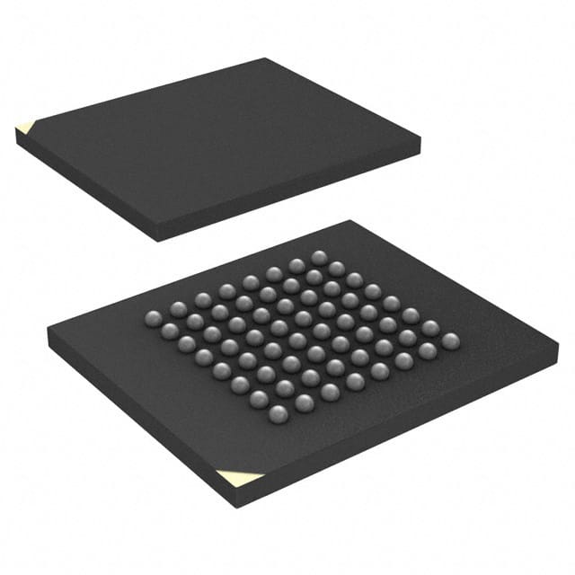
PC28F128J3F75A
Overview
- Category: Flash Memory
- Use: Data storage in electronic devices
- Characteristics:
- High capacity
- Non-volatile memory
- Fast read and write speeds
- Reliable and durable
- Package: Integrated Circuit (IC)
- Essence: Stores digital information in a compact and portable form
- Packaging/Quantity: Typically sold individually or in bulk packs
Specifications
- Capacity: 128 gigabytes (GB)
- Interface: Parallel
- Voltage: 2.7V - 3.6V
- Access Time: 75 nanoseconds (ns)
- Operating Temperature: -40°C to +85°C
- Erase/Program Cycles: 100,000 cycles
Pin Configuration
The PC28F128J3F75A has a total of 48 pins. The pin configuration is as follows:
- VCC
- A0
- A1
- A2
- A3
- A4
- A5
- A6
- A7
- A8
- A9
- A10
- A11
- A12
- A13
- A14
- A15
- A16
- A17
- A18
- A19
- A20
- A21
- A22
- A23
- A24
- A25
- A26
- A27
- A28
- A29
- A30
- A31
- DQ0
- DQ1
- DQ2
- DQ3
- DQ4
- DQ5
- DQ6
- DQ7
- WE#
- CE#
- RE#
- WP#
- RY/BY#
- VSS
- NC
Functional Features
- High-speed data transfer
- Reliable data retention
- Efficient erase and program operations
- Built-in error correction mechanisms
- Low power consumption
- Support for various memory management techniques
Advantages
- Large storage capacity
- Fast read and write speeds
- Long lifespan
- Compact and lightweight design
- Compatibility with a wide range of devices
- Easy integration into existing systems
Disadvantages
- Relatively high cost compared to other storage options
- Limited number of erase/program cycles
- Susceptible to physical damage if mishandled
- Requires specialized programming equipment for initial setup
Working Principles
The PC28F128J3F75A utilizes a technology called NAND flash memory. It stores digital information by trapping electric charges in floating gate transistors. These charges represent binary data (0s and 1s). When reading data, the charges are measured to determine the stored information. During writing or erasing, the charges are added or removed from the floating gates.
Detailed Application Field Plans
The PC28F128J3F75A is commonly used in various electronic devices, including:
- Solid-state drives (SSDs)
- Digital cameras
- Mobile phones
- Tablets
- Gaming consoles
- Embedded systems
- Industrial control systems
Its high capacity and fast access times make it suitable for applications that require large amounts of data storage and quick retrieval.
Alternative Models
- PC28F128J3F75B: Similar specifications but with higher operating temperature range (-40°C to +105°C).
- PC28F128J3F75C: Similar specifications but with lower power consumption.
- PC28F128J3F75D: Similar specifications but with higher erase/program cycles (500,000 cycles).
These alternative models provide options for different temperature requirements, power constraints, and durability needs.
In conclusion, the PC28F128J3F75A is a high-capacity flash memory device used for data storage in various electronic devices. Its fast read and write speeds, reliability, and compact design make it a popular choice in the industry. However, it has some limitations such as limited erase/program cycles and higher cost compared to other storage options. Nonetheless, its working principles and versatile application field plans make it an essential component in modern technology.
Enumere 10 preguntas y respuestas comunes relacionadas con la aplicación de PC28F128J3F75A en soluciones técnicas
Sure! Here are 10 common questions and answers related to the application of PC28F128J3F75A in technical solutions:
Q: What is PC28F128J3F75A? A: PC28F128J3F75A is a specific model of flash memory chip manufactured by Intel.
Q: What is the storage capacity of PC28F128J3F75A? A: PC28F128J3F75A has a storage capacity of 128 megabytes (MB).
Q: What is the interface used to connect PC28F128J3F75A to a system? A: PC28F128J3F75A uses a parallel NOR flash interface.
Q: What voltage does PC28F128J3F75A operate at? A: PC28F128J3F75A operates at a voltage range of 2.7V to 3.6V.
Q: Can PC28F128J3F75A be used in industrial applications? A: Yes, PC28F128J3F75A is suitable for use in industrial applications due to its reliability and durability.
Q: Is PC28F128J3F75A compatible with other flash memory chips? A: PC28F128J3F75A follows industry-standard protocols and can be used alongside other compatible flash memory chips.
Q: What is the maximum operating temperature of PC28F128J3F75A? A: PC28F128J3F75A can operate reliably in temperatures ranging from -40°C to +85°C.
Q: Does PC28F128J3F75A support hardware encryption? A: No, PC28F128J3F75A does not have built-in hardware encryption capabilities.
Q: Can PC28F128J3F75A be used in automotive applications? A: Yes, PC28F128J3F75A is suitable for use in automotive applications due to its temperature range and reliability.
Q: What is the expected lifespan of PC28F128J3F75A? A: PC28F128J3F75A has a typical lifespan of 100,000 program/erase cycles, ensuring long-term data retention.
Please note that these answers are general and may vary depending on specific application requirements and datasheet specifications.