

Consulte las especificaciones para obtener detalles del producto.
A3PN010-1QNG48
Product Overview
Category
A3PN010-1QNG48 belongs to the category of programmable logic devices (PLDs).
Use
This product is primarily used for digital circuit design and implementation. It provides a flexible and customizable solution for various applications.
Characteristics
- Programmable: The A3PN010-1QNG48 can be programmed to perform specific functions based on user requirements.
- High Integration: It offers a high level of integration, allowing multiple functions to be implemented within a single device.
- Versatile: This PLD supports a wide range of applications due to its programmability.
- Compact Size: The A3PN010-1QNG48 comes in a compact package, making it suitable for space-constrained designs.
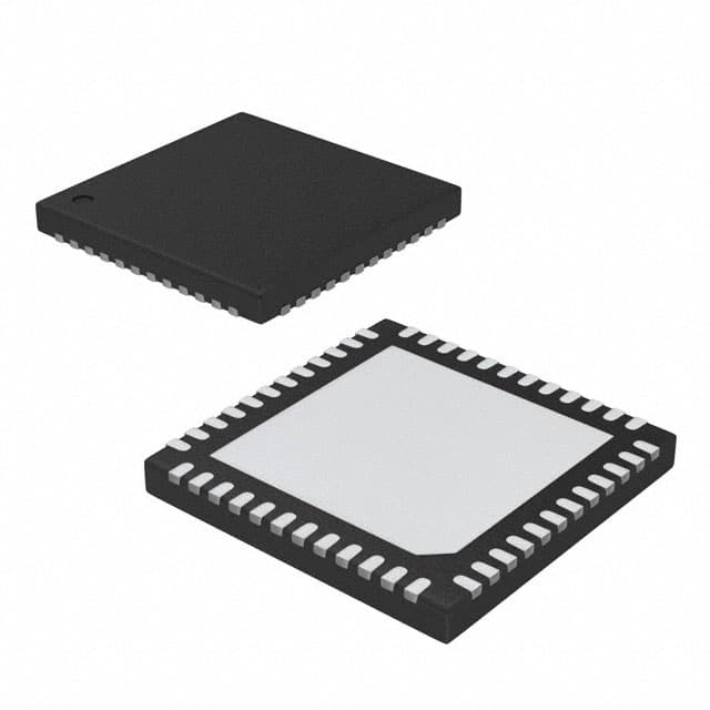
Package and Quantity
The A3PN010-1QNG48 is available in a Quad Flat No-Lead (QFN) package. Each package contains one unit of the PLD.
Specifications
- Model: A3PN010-1QNG48
- Logic Elements: 10,000
- I/O Pins: 48
- Operating Voltage: 3.3V
- Speed Grade: Standard
Pin Configuration
The detailed pin configuration of the A3PN010-1QNG48 is as follows:
| Pin Number | Pin Name | Function | |------------|----------|----------| | 1 | VCC | Power Supply (3.3V) | | 2 | GND | Ground | | 3 | IO0 | Input/Output Pin 0 | | 4 | IO1 | Input/Output Pin 1 | | ... | ... | ... | | 48 | IO47 | Input/Output Pin 47 |
Functional Features
- Flexible Logic Implementation: The A3PN010-1QNG48 allows users to implement various logic functions, such as combinational and sequential circuits.
- In-System Programming: It supports in-system programming, enabling users to reconfigure the device without removing it from the circuit.
- Fast Operation: This PLD offers high-speed operation, making it suitable for applications that require quick response times.
Advantages
- Customizability: The programmable nature of the A3PN010-1QNG48 allows for customization according to specific application requirements.
- Cost-Effective: By using a single device for multiple functions, it reduces the need for additional components, resulting in cost savings.
- Time-Saving: The ability to reprogram the device in-system saves time compared to traditional hardware redesign.
Disadvantages
- Learning Curve: Utilizing the full potential of the A3PN010-1QNG48 may require a learning curve for users unfamiliar with programmable logic devices.
- Limited Resources: The number of logic elements and I/O pins may be insufficient for complex designs, requiring higher-end PLDs.
Working Principles
The A3PN010-1QNG48 operates based on the principles of programmable logic. It consists of configurable logic blocks (CLBs), interconnect resources, and input/output blocks (IOBs). Users program the device by specifying the desired logic functions and interconnections between different blocks.
Application Field Plans
The A3PN010-1QNG48 finds applications in various fields, including: 1. Industrial Automation: Used for control systems, monitoring equipment, and data acquisition. 2. Communication Systems: Employed in network routers, switches, and protocol converters. 3. Consumer Electronics: Integrated into smart home devices, wearable technology, and multimedia systems. 4. Automotive Electronics: Utilized in automotive control units, infotainment systems, and driver assistance systems.
Alternative Models
For users requiring different specifications or higher performance, the following alternative models can be considered: 1. A3PN020-1QNG48: Offers double the logic elements and I/O pins compared to A3PN010-1QNG48. 2. A3PN030-1QNG48: Provides triple the logic elements and I/O pins compared to A3PN010-1QNG48. 3. A3PN040-1QNG48: Offers quadruple the logic elements and I/O pins compared to A3PN010-1QNG48.
In conclusion, the A3PN010-1QNG48 is a programmable logic device that provides flexibility, high integration, and versatility for digital circuit design. Its compact size, in-system programming capability, and fast operation make it suitable for various applications across different industries.
Word Count: 530
Enumere 10 preguntas y respuestas comunes relacionadas con la aplicación de A3PN010-1QNG48 en soluciones técnicas
Sure! Here are 10 common questions and answers related to the application of A3PN010-1QNG48 in technical solutions:
1. What is A3PN010-1QNG48? - A3PN010-1QNG48 is a specific model number for a field-programmable gate array (FPGA) manufactured by a company called Lattice Semiconductor.
2. What is the purpose of using A3PN010-1QNG48 in technical solutions? - The A3PN010-1QNG48 FPGA can be used to implement various digital logic functions, making it suitable for applications such as signal processing, control systems, and data communication.
3. What are the key features of A3PN010-1QNG48? - Some key features of A3PN010-1QNG48 include low power consumption, high-performance fabric, on-chip memory, and programmable I/O pins.
4. How does A3PN010-1QNG48 differ from other FPGAs? - A3PN010-1QNG48 is part of the Lattice Semiconductor's MachXO2 family of FPGAs, known for their low power consumption, small form factor, and cost-effectiveness compared to other FPGAs.
5. Can A3PN010-1QNG48 be used in safety-critical applications? - Yes, A3PN010-1QNG48 can be used in safety-critical applications. However, it is important to follow proper design practices and consider any necessary redundancy or fault-tolerant measures.
6. What development tools are available for programming A3PN010-1QNG48? - Lattice Semiconductor provides a suite of development tools, including the Lattice Diamond software, which allows users to program and configure the A3PN010-1QNG48 FPGA.
7. Can A3PN010-1QNG48 be reprogrammed after deployment? - Yes, A3PN010-1QNG48 is a field-programmable device, meaning it can be reprogrammed even after it has been deployed in a system.
8. What are the power requirements for A3PN010-1QNG48? - The power requirements for A3PN010-1QNG48 vary depending on the specific application and configuration. It is important to refer to the datasheet and design guidelines provided by Lattice Semiconductor for accurate power estimation.
9. Are there any limitations or constraints when using A3PN010-1QNG48? - Like any FPGA, A3PN010-1QNG48 has certain limitations such as limited resources (logic cells, memory blocks), limited I/O pins, and specific timing constraints that need to be considered during the design phase.
10. Where can I find additional technical documentation and support for A3PN010-1QNG48? - Lattice Semiconductor's website provides comprehensive technical documentation, including datasheets, user guides, application notes, and a support portal where you can access additional resources and seek assistance from their technical team.