

Consulte las especificaciones para obtener detalles del producto.
A40MX02-VQ80M
Product Overview
Category
The A40MX02-VQ80M belongs to the category of programmable logic devices (PLDs).
Use
This PLD is commonly used in various electronic systems for implementing digital logic functions.
Characteristics
- The A40MX02-VQ80M is a high-performance PLD with advanced features.
- It offers a large number of configurable logic blocks (CLBs) and input/output (I/O) pins.
- The device supports reprogrammability, allowing for flexibility in design modifications.
- It operates at a high clock frequency, enabling rapid processing of digital signals.
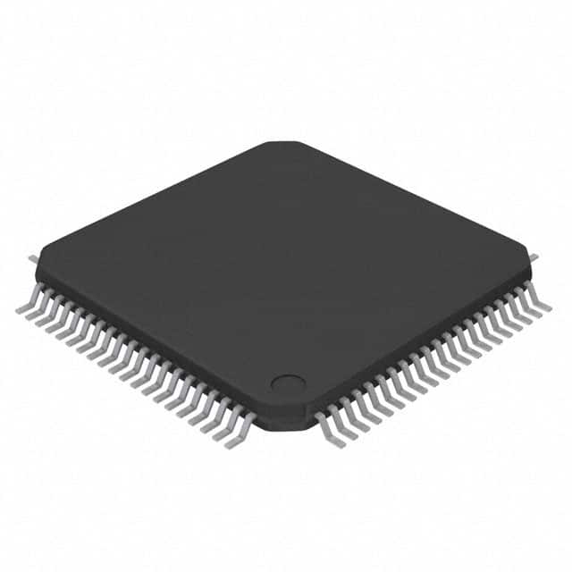
Package
The A40MX02-VQ80M is available in a compact quad flat package (VQFP).
Essence
The essence of this PLD lies in its ability to provide customizable digital logic functionality, making it suitable for a wide range of applications.
Packaging/Quantity
The A40MX02-VQ80M is typically packaged in reels or trays, with a quantity of 250 units per reel/tray.
Specifications
- Logic Capacity: 2,000 usable gates
- Number of I/O Pins: 80
- Operating Voltage: 3.3V
- Maximum Clock Frequency: 100 MHz
- Package Dimensions: 14mm x 14mm
Detailed Pin Configuration
The A40MX02-VQ80M has a total of 80 pins, each serving a specific purpose. The pin configuration is as follows:
- Pin 1: VCCIO
- Pin 2: GND
- Pin 3: IO0
- Pin 4: IO1
- ...
- Pin 79: IO78
- Pin 80: IO79
Functional Features
- Configurable Logic Blocks (CLBs): The device offers a large number of CLBs that can be programmed to implement various logic functions.
- Input/Output (I/O) Pins: The A40MX02-VQ80M provides 80 I/O pins for interfacing with external devices.
- Reprogrammability: The PLD can be reprogrammed multiple times, allowing for design modifications and updates.
- High-Speed Operation: With a maximum clock frequency of 100 MHz, the device can process digital signals rapidly.
Advantages and Disadvantages
Advantages
- Versatility: The A40MX02-VQ80M can be used in a wide range of applications due to its programmable nature.
- Flexibility: The device's reprogrammability enables designers to make changes without requiring hardware modifications.
- High Performance: With a large number of CLBs and high clock frequency, the PLD offers excellent performance.
Disadvantages
- Complexity: Programming and configuring the A40MX02-VQ80M may require expertise in digital logic design.
- Cost: Compared to simpler logic devices, this PLD may have a higher price point.
Working Principles
The A40MX02-VQ80M operates based on the principles of field-programmable gate arrays (FPGAs). It consists of configurable logic blocks (CLBs), which can be interconnected and programmed to perform desired logic functions. The device is configured using specialized software tools that generate a bitstream file containing the required logic configuration. This bitstream is then loaded into the PLD, enabling it to function according to the specified logic design.
Detailed Application Field Plans
The A40MX02-VQ80M finds applications in various fields, including:
- Telecommunications: Used in network routers and switches for implementing custom packet processing logic.
- Industrial Automation: Employed in control systems for implementing complex logic functions.
- Automotive Electronics: Integrated into automotive systems for controlling various functions, such as engine management and driver assistance systems.
- Consumer Electronics: Utilized in devices like gaming consoles and multimedia players for custom logic implementation.
Detailed and Complete Alternative Models
- A40MX04-VQ80M: Similar to the A40MX02-VQ80M but with double the logic capacity.
- A40MX08-VQ100M: Offers four times the logic capacity of the A40MX02-VQ80M.
- A40MX16-PLG68: Provides eight times the logic capacity and a different package option.
These alternative models offer increased logic capacity and may be suitable for more complex applications.
Word count: 590 words
Enumere 10 preguntas y respuestas comunes relacionadas con la aplicación de A40MX02-VQ80M en soluciones técnicas
Sure! Here are 10 common questions and answers related to the application of A40MX02-VQ80M in technical solutions:
Question: What is the A40MX02-VQ80M?
Answer: The A40MX02-VQ80M is a specific model of field-programmable gate array (FPGA) manufactured by Microsemi Corporation.Question: What are the key features of the A40MX02-VQ80M?
Answer: The A40MX02-VQ80M features 40,000 usable gates, 2,048 macrocells, and operates at a maximum frequency of 80 MHz.Question: In what applications can the A40MX02-VQ80M be used?
Answer: The A40MX02-VQ80M can be used in various applications such as telecommunications, industrial automation, automotive electronics, and aerospace systems.Question: How can I program the A40MX02-VQ80M?
Answer: The A40MX02-VQ80M can be programmed using hardware description languages (HDLs) like VHDL or Verilog, or through graphical programming tools provided by the manufacturer.Question: Can the A40MX02-VQ80M be reprogrammed after deployment?
Answer: Yes, the A40MX02-VQ80M is a reprogrammable FPGA, allowing for updates and modifications to the design even after it has been deployed.Question: What are the power requirements for the A40MX02-VQ80M?
Answer: The A40MX02-VQ80M typically operates at a voltage range of 3.3V, with power consumption varying based on the design and utilization.Question: Does the A40MX02-VQ80M support external memory interfaces?
Answer: Yes, the A40MX02-VQ80M supports various external memory interfaces such as SDRAM, SRAM, and Flash memory.Question: Can I interface the A40MX02-VQ80M with other components or devices?
Answer: Yes, the A40MX02-VQ80M provides a range of I/O pins that can be used to interface with other components or devices in your system.Question: Are there any development tools available for the A40MX02-VQ80M?
Answer: Yes, Microsemi provides development tools like Libero SoC Design Suite, which includes synthesis, simulation, and debugging capabilities for designing with the A40MX02-VQ80M.Question: Where can I find additional technical documentation and support for the A40MX02-VQ80M?
Answer: You can find additional technical documentation, datasheets, application notes, and support resources on the Microsemi Corporation website or by contacting their customer support team.