

Consulte las especificaciones para obtener detalles del producto.
A54SX32A-2FG256I
Product Overview
Category
The A54SX32A-2FG256I belongs to the category of Field Programmable Gate Arrays (FPGAs).
Use
FPGAs are integrated circuits that can be programmed and reprogrammed to perform various digital functions. The A54SX32A-2FG256I is specifically designed for applications requiring high-performance logic integration.
Characteristics
- High-performance FPGA with 54,000 system gates
- 32,768 programmable logic cells
- Advanced architecture for efficient implementation of complex designs
- Low power consumption
- Fast configuration time
- Wide range of I/O options
- Robust design for reliable operation in demanding environments
Package
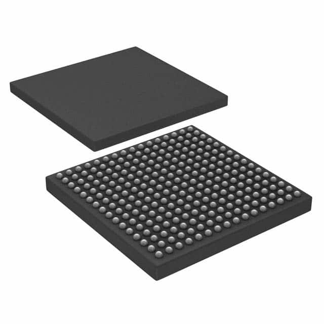
The A54SX32A-2FG256I comes in a 256-pin Fine-Pitch Ball Grid Array (FBGA) package.
Essence
The essence of the A54SX32A-2FG256I lies in its ability to provide flexible and customizable digital logic functionality, allowing designers to implement complex systems on a single chip.
Packaging/Quantity
The A54SX32A-2FG256I is typically packaged individually and is available in various quantities depending on the customer's requirements.
Specifications
- System Gates: 54,000
- Logic Cells: 32,768
- I/O Pins: 256
- Operating Voltage: 1.8V
- Maximum Frequency: 300 MHz
- Configuration Memory: 4 Mb Flash EEPROM
- On-Chip RAM: 512 Kb
Detailed Pin Configuration
The A54SX32A-2FG256I has 256 pins, each serving a specific purpose in the overall functionality of the FPGA. The detailed pin configuration can be found in the product datasheet.
Functional Features
- High-density programmable logic cells for complex designs
- Flexible I/O options for interfacing with external devices
- Efficient routing architecture for optimized signal propagation
- On-chip memory resources for data storage and processing
- Built-in clock management circuitry for precise timing control
- Support for various communication protocols
Advantages and Disadvantages
Advantages
- High-performance FPGA suitable for demanding applications
- Flexibility to implement custom logic functions
- Fast configuration time enables rapid prototyping
- Low power consumption for energy-efficient designs
- Robust design ensures reliable operation in harsh environments
Disadvantages
- Steep learning curve for beginners due to the complexity of FPGA programming
- Limited availability of alternative models with similar specifications
- Higher cost compared to other programmable logic devices
Working Principles
The A54SX32A-2FG256I operates based on the principles of reconfigurable digital logic. It consists of a matrix of programmable logic cells interconnected through configurable routing resources. The user programs the FPGA by specifying the desired logic functions and interconnections using a Hardware Description Language (HDL). Upon configuration, the FPGA executes the programmed logic, enabling the desired functionality.
Detailed Application Field Plans
The A54SX32A-2FG256I finds applications in various fields, including:
- Telecommunications: Used in base stations, network switches, and routers for high-speed data processing.
- Industrial Automation: Employed in control systems, motor drives, and robotics for real-time control and monitoring.
- Aerospace and Defense: Utilized in radar systems, avionics, and military-grade equipment for reliable and secure operation.
- Medical Devices: Integrated into medical imaging systems, patient monitoring devices, and diagnostic equipment for data processing and analysis.
- Automotive: Applied in advanced driver assistance systems (ADAS), infotainment systems, and engine control units for enhanced vehicle performance and safety.
Detailed and Complete Alternative Models
While the A54SX32A-2FG256I offers unique features, there are alternative FPGA models available with similar capabilities. Some notable alternatives include:
- Xilinx Spartan-6 XC6SLX45: Offers comparable logic capacity and I/O options.
- Intel Cyclone IV EP4CE115: Provides similar performance and power characteristics.
- Lattice ECP5-85: Offers a different architecture but comparable functionality for certain applications.
These alternative models can be considered based on specific project requirements and design constraints.
Word count: 550 words
Enumere 10 preguntas y respuestas comunes relacionadas con la aplicación de A54SX32A-2FG256I en soluciones técnicas
Sure! Here are 10 common questions and answers related to the application of A54SX32A-2FG256I in technical solutions:
1. What is the A54SX32A-2FG256I? The A54SX32A-2FG256I is a specific model of field-programmable gate array (FPGA) manufactured by Microsemi Corporation.
2. What are the key features of the A54SX32A-2FG256I? Some key features of this FPGA include 54,000 system gates, 32,768 macrocells, 288 I/O pins, and a 2.5V core voltage.
3. What are the typical applications of the A54SX32A-2FG256I? This FPGA is commonly used in various technical solutions such as telecommunications, industrial automation, automotive electronics, medical devices, and aerospace systems.
4. How can I program the A54SX32A-2FG256I? You can program this FPGA using hardware description languages (HDLs) like VHDL or Verilog, along with design software tools provided by Microsemi.
5. What is the power consumption of the A54SX32A-2FG256I? The power consumption of this FPGA depends on the specific design and usage scenario. It is recommended to refer to the datasheet for detailed power consumption information.
6. Can I reprogram the A54SX32A-2FG256I after it has been deployed in a system? Yes, FPGAs are known for their reprogrammability. You can reprogram the A54SX32A-2FG256I multiple times to update or modify its functionality.
7. Are there any development boards available for the A54SX32A-2FG256I? Yes, Microsemi offers development boards specifically designed for the A54SX32A-2FG256I, which provide a convenient platform for prototyping and testing.
8. What is the maximum operating frequency of the A54SX32A-2FG256I? The maximum operating frequency of this FPGA depends on various factors like design complexity and external constraints. It is recommended to refer to the datasheet for specific details.
9. Can I interface the A54SX32A-2FG256I with other components or devices? Yes, this FPGA provides a wide range of I/O pins that can be used to interface with other components or devices such as sensors, memory modules, communication interfaces, and more.
10. Are there any application notes or reference designs available for the A54SX32A-2FG256I? Yes, Microsemi provides application notes, reference designs, and technical documentation to assist users in implementing the A54SX32A-2FG256I in their specific applications. These resources can be found on their official website or support portal.
Please note that the answers provided here are general and may vary depending on the specific requirements and use cases. It is always recommended to refer to the official documentation and consult with experts for accurate and detailed information.