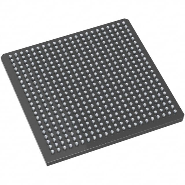
Consulte las especificaciones para obtener detalles del producto.

AFS600-2FGG484I
Product Overview
Category
AFS600-2FGG484I belongs to the category of Field Programmable Gate Arrays (FPGAs).
Use
This product is primarily used in digital logic circuits for various applications such as telecommunications, automotive electronics, consumer electronics, and industrial automation.
Characteristics
- High flexibility and reconfigurability
- Large number of programmable logic blocks
- High-speed performance
- Low power consumption
- Integration of various functions on a single chip
Package
The AFS600-2FGG484I FPGA is available in a 484-pin Fine-Pitch Ball Grid Array (FBGA) package.
Essence
The essence of AFS600-2FGG484I lies in its ability to provide a highly customizable and versatile solution for implementing complex digital logic circuits.
Packaging/Quantity
The AFS600-2FGG484I FPGA is typically packaged individually and is available in various quantities depending on customer requirements.
Specifications
- Logic Elements: 600,000
- Embedded Memory: 1,500 Kbits
- Maximum Number of User I/Os: 400
- Clock Management Tiles: 20
- DSP Blocks: 360
- Maximum Operating Frequency: 500 MHz
- Operating Voltage: 1.2V
- Package Type: FBGA
- Package Pins: 484
Detailed Pin Configuration
The detailed pin configuration of AFS600-2FGG484I can be found in the product datasheet provided by the manufacturer.
Functional Features
- High-performance programmable logic blocks
- Flexible clock management resources
- Dedicated digital signal processing blocks
- On-chip memory blocks for data storage
- Various I/O standards and interfaces
- Built-in configuration memory for easy reprogramming
Advantages and Disadvantages
Advantages
- High flexibility and reconfigurability allow for rapid prototyping and design iterations.
- Integration of multiple functions on a single chip reduces the need for additional components.
- Low power consumption makes it suitable for battery-powered devices.
- High-speed performance enables real-time processing of complex algorithms.
Disadvantages
- Initial development cost can be higher compared to fixed-function ASICs.
- Limited resources may restrict the complexity of designs that can be implemented.
- FPGA programming requires specialized knowledge and tools.
Working Principles
AFS600-2FGG484I is based on the principle of configurable logic blocks (CLBs) interconnected through programmable routing resources. The CLBs consist of look-up tables, flip-flops, and other components that can be configured to implement desired logic functions. The interconnect resources allow for flexible routing of signals between different CLBs, enabling the creation of complex digital circuits.
Detailed Application Field Plans
The AFS600-2FGG484I FPGA finds applications in various fields, including:
- Telecommunications: Used in base stations, network switches, and routers for high-speed data processing and protocol handling.
- Automotive Electronics: Employed in advanced driver-assistance systems (ADAS), engine control units (ECUs), and infotainment systems for enhanced functionality and performance.
- Consumer Electronics: Utilized in smart TVs, gaming consoles, and multimedia devices for video and audio processing, as well as user interface implementation.
- Industrial Automation: Applied in programmable logic controllers (PLCs), motor control systems, and robotics for precise control and automation tasks.
Detailed and Complete Alternative Models
- AFS400-1FGG256I: A lower-density FPGA with 400,000 logic elements and 256-pin FBGA package.
- AFS1200-3FGG900I: A higher-density FPGA with 1.2 million logic elements and 900-pin FBGA package.
- AFS200-2FGG484I: A mid-range FPGA with 200,000 logic elements and 484-pin FBGA package.
These alternative models provide different options based on the required logic density and pin count.
Word Count: 540 words
Enumere 10 preguntas y respuestas comunes relacionadas con la aplicación de AFS600-2FGG484I en soluciones técnicas
Sure! Here are 10 common questions and answers related to the application of AFS600-2FGG484I in technical solutions:
Q: What is AFS600-2FGG484I? A: AFS600-2FGG484I is a specific model of Field Programmable Gate Array (FPGA) manufactured by a company called Achronix Semiconductor.
Q: What are the key features of AFS600-2FGG484I? A: Some key features of AFS600-2FGG484I include high-performance programmable logic, embedded memory blocks, high-speed I/O interfaces, and low power consumption.
Q: In what technical solutions can AFS600-2FGG484I be used? A: AFS600-2FGG484I can be used in various technical solutions such as data center acceleration, artificial intelligence, machine learning, networking, and high-performance computing.
Q: How does AFS600-2FGG484I contribute to data center acceleration? A: AFS600-2FGG484I provides high-performance programmable logic that can be customized to accelerate specific tasks like data processing, encryption/decryption, or compression/decompression in data centers.
Q: Can AFS600-2FGG484I be used for artificial intelligence applications? A: Yes, AFS600-2FGG484I can be utilized in AI applications for tasks like neural network inference, deep learning, and real-time analytics due to its high-performance capabilities.
Q: What advantages does AFS600-2FGG484I offer in networking solutions? A: AFS600-2FGG484I enables the implementation of custom networking protocols, packet processing, and traffic management algorithms, leading to improved network performance and flexibility.
Q: How does AFS600-2FGG484I support high-performance computing? A: AFS600-2FGG484I provides high-speed I/O interfaces and customizable logic that can be tailored to specific computational tasks, making it suitable for demanding HPC applications.
Q: Can AFS600-2FGG484I be programmed using industry-standard design tools? A: Yes, AFS600-2FGG484I can be programmed using popular design tools like Xilinx Vivado or Intel Quartus Prime, ensuring compatibility with existing FPGA development workflows.
Q: What is the power consumption of AFS600-2FGG484I? A: The power consumption of AFS600-2FGG484I varies depending on the specific configuration and workload but is generally designed to be energy-efficient compared to alternative solutions.
Q: Are there any specific application examples where AFS600-2FGG484I has been successfully deployed? A: Yes, AFS600-2FGG484I has been used in various real-world applications such as cloud computing acceleration, autonomous vehicles, video processing, and financial analytics.
Please note that the answers provided here are general and may vary based on specific use cases and requirements.

