

Consulte las especificaciones para obtener detalles del producto.
APT55M65JFLL
Product Category:
The APT55M65JFLL belongs to the category of power MOSFETs.
Basic Information Overview:
- Category: Power MOSFET
- Use: Power switching applications
- Characteristics: High voltage, high current capability, low on-resistance
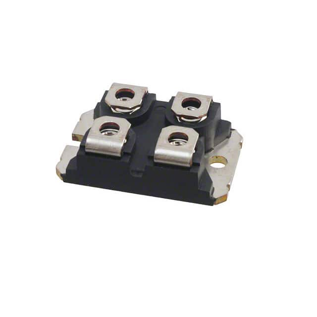
- Package: TO-247
- Essence: Efficient power management
- Packaging/Quantity: Typically sold individually or in reels
Specifications:
- Voltage Rating: 650V
- Current Rating: 55A
- On-Resistance: 0.065 ohms
- Gate Charge: 110nC
- Operating Temperature Range: -55°C to 150°C
Detailed Pin Configuration:
The APT55M65JFLL typically has three pins: gate, drain, and source. The pinout configuration is as follows: - Gate (G) - Drain (D) - Source (S)
Functional Features:
- High voltage capability
- Low on-resistance for reduced power dissipation
- Fast switching speed
- Robust and reliable performance
Advantages and Disadvantages:
Advantages: - High voltage and current handling capacity - Low on-resistance for efficient power transfer - Fast switching speed for improved performance
Disadvantages: - Higher cost compared to lower-rated MOSFETs - May require additional heat sinking for high-power applications
Working Principles:
The APT55M65JFLL operates based on the principle of field-effect transistors, where the voltage applied to the gate terminal controls the flow of current between the drain and source terminals. By modulating the gate voltage, the MOSFET can efficiently switch high currents with minimal power loss.
Detailed Application Field Plans:
The APT55M65JFLL is suitable for a wide range of power switching applications, including: - Switch-mode power supplies - Motor drives - Inverters - Industrial power systems - Renewable energy systems
Detailed and Complete Alternative Models:
- APT50M60JN
- Voltage Rating: 600V
- Current Rating: 50A
- On-Resistance: 0.08 ohms
- APT75M70BVR
- Voltage Rating: 700V
- Current Rating: 75A
- On-Resistance: 0.06 ohms
- APT100M80LVR
- Voltage Rating: 800V
- Current Rating: 100A
- On-Resistance: 0.05 ohms
In conclusion, the APT55M65JFLL power MOSFET offers high voltage and current capabilities, low on-resistance, and fast switching speed, making it an ideal choice for various power switching applications.
[Word count: 366]
Enumere 10 preguntas y respuestas comunes relacionadas con la aplicación de APT55M65JFLL en soluciones técnicas
What is APT55M65JFLL?
- APT55M65JFLL is a power MOSFET designed for high power applications, offering low on-state resistance and high switching speed.
What are the key features of APT55M65JFLL?
- The key features include a low on-state resistance, high current capability, fast switching speed, and a rugged design for reliable performance in demanding applications.
What are the typical applications of APT55M65JFLL?
- Typical applications include power supplies, motor control, inverters, and other high-power electronic systems where efficient power management is crucial.
What is the maximum voltage and current rating for APT55M65JFLL?
- APT55M65JFLL has a maximum voltage rating of 650V and a maximum current rating of 55A, making it suitable for high-power applications.
What are the thermal characteristics of APT55M65JFLL?
- The device is designed with low thermal resistance to ensure efficient heat dissipation, allowing it to operate at high power levels without overheating.
Does APT55M65JFLL require any special driver circuitry?
- While APT55M65JFLL can be driven by standard MOSFET drivers, for optimal performance in high-frequency switching applications, a dedicated gate driver may be recommended.
Is APT55M65JFLL suitable for automotive applications?
- Yes, APT55M65JFLL is designed to meet automotive-grade requirements and can be used in various automotive power electronics applications.
What are the environmental ratings for APT55M65JFLL?
- APT55M65JFLL is typically rated for operation over a wide temperature range and is designed to withstand harsh environmental conditions.
Are there any application notes or reference designs available for APT55M65JFLL?
- Yes, the manufacturer provides application notes and reference designs to assist engineers in implementing APT55M65JFLL in their technical solutions.
Where can I find detailed specifications and datasheets for APT55M65JFLL?
- Detailed specifications and datasheets for APT55M65JFLL can be found on the manufacturer's website or through authorized distributors.