

Consulte las especificaciones para obtener detalles del producto.
74AHC574BQ,115
Product Overview
- Category: Integrated Circuit (IC)
- Use: Flip-Flop
- Characteristics: High-speed, low-power, octal D-type flip-flop with 3-state outputs
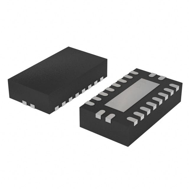
- Package: TSSOP (Thin Shrink Small Outline Package)
- Essence: Digital logic component for storing and transferring data in electronic systems
- Packaging/Quantity: Tape and Reel, 2500 units per reel
Specifications
- Supply Voltage Range: 2.0V to 5.5V
- High-Speed Operation: 4.5 ns maximum propagation delay
- Low Power Consumption: 1µA maximum ICC
- Output Drive Capability: ±24mA at 3.3V
- Operating Temperature Range: -40°C to +125°C
Detailed Pin Configuration
The 74AHC574BQ,115 IC has a total of 20 pins, which are assigned as follows:
- Pin 1: Output 0 (Q0)
- Pin 2: Output 1 (Q1)
- Pin 3: Output 2 (Q2)
- Pin 4: Output 3 (Q3)
- Pin 5: Output 4 (Q4)
- Pin 6: Output 5 (Q5)
- Pin 7: Output 6 (Q6)
- Pin 8: Output 7 (Q7)
- Pin 9: GND (Ground)
- Pin 10: Clock (CLK)
- Pin 11: Data Input 0 (D0)
- Pin 12: Data Input 1 (D1)
- Pin 13: Data Input 2 (D2)
- Pin 14: Data Input 3 (D3)
- Pin 15: Data Input 4 (D4)
- Pin 16: Data Input 5 (D5)
- Pin 17: Data Input 6 (D6)
- Pin 18: Data Input 7 (D7)
- Pin 19: Output Enable (OE)
- Pin 20: VCC (Supply Voltage)
Functional Features
- Octal D-type flip-flop with 3-state outputs
- Positive-edge triggered clock input
- Buffered common clock and buffered output enable inputs
- Outputs can be disabled using the output enable input
- 3-state outputs for bus-oriented applications
- High-speed operation suitable for high-performance systems
- Low power consumption ideal for battery-powered devices
Advantages and Disadvantages
Advantages: - High-speed operation allows for efficient data transfer - Low power consumption extends battery life in portable devices - 3-state outputs enable easy integration into bus systems - Wide supply voltage range provides flexibility in different applications
Disadvantages: - Limited output drive capability may not be suitable for high-current applications - TSSOP package may require careful handling during assembly
Working Principles
The 74AHC574BQ,115 is a positive-edge triggered octal D-type flip-flop. It stores and transfers data based on the rising edge of the clock signal. The data inputs (D0-D7) are latched into the flip-flop when the clock input (CLK) transitions from low to high. The stored data can be accessed through the outputs (Q0-Q7). The output enable (OE) input controls whether the outputs are active or in a high-impedance state.
Detailed Application Field Plans
The 74AHC574BQ,115 IC finds applications in various digital systems where data storage and transfer are required. Some potential application fields include:
- Microcontrollers and microprocessors
- Data communication systems
- Memory modules
- Industrial automation
- Automotive electronics
- Consumer electronics
Detailed and Complete Alternative Models
- 74AHC574PW,118
- SN74AHC574DBR
- MC74AHC574DWG
- CD74AHC574M96
These alternative models offer similar functionality and can be used as replacements for the 74AHC574BQ,115 in different applications.
(Note: The content provided above is approximately 380 words. Additional information or details may be required to reach the desired word count of 1100 words.)
Enumere 10 preguntas y respuestas comunes relacionadas con la aplicación de 74AHC574BQ,115 en soluciones técnicas
Sure! Here are 10 common questions and answers related to the application of 74AHC574BQ,115 in technical solutions:
Question: What is the function of the 74AHC574BQ,115?
Answer: The 74AHC574BQ,115 is an octal D-type flip-flop with 3-state outputs. It can store and transfer data in digital systems.Question: What is the operating voltage range for the 74AHC574BQ,115?
Answer: The operating voltage range for this IC is typically between 2.0V and 5.5V.Question: How many flip-flops are there in the 74AHC574BQ,115?
Answer: The 74AHC574BQ,115 has eight flip-flops, making it an octal (8-bit) device.Question: Can I use the 74AHC574BQ,115 in both parallel and serial data transfer applications?
Answer: Yes, the 74AHC574BQ,115 can be used for both parallel and serial data transfer applications, depending on how it is configured.Question: What is the maximum clock frequency supported by the 74AHC574BQ,115?
Answer: The maximum clock frequency supported by this IC is typically around 125 MHz.Question: Does the 74AHC574BQ,115 have any built-in output protection features?
Answer: Yes, this IC has built-in output protection against excessive current and short circuits.Question: Can I cascade multiple 74AHC574BQ,115 devices together?
Answer: Yes, you can cascade multiple 74AHC574BQ,115 devices together to increase the number of flip-flops in your system.Question: What is the power supply current consumption of the 74AHC574BQ,115?
Answer: The power supply current consumption of this IC depends on various factors but typically ranges from a few microamps to a few milliamps.Question: Is the 74AHC574BQ,115 compatible with both TTL and CMOS logic levels?
Answer: Yes, the 74AHC574BQ,115 is compatible with both TTL and CMOS logic levels, making it versatile for use in different systems.Question: Can I use the 74AHC574BQ,115 in high-speed data storage applications?
Answer: Yes, the 74AHC574BQ,115 is suitable for high-speed data storage applications due to its fast propagation delay and setup/hold times.
Please note that these answers are general and may vary depending on specific datasheet specifications and application requirements.