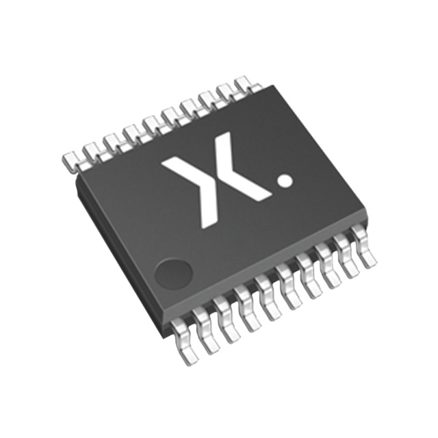
Consulte las especificaciones para obtener detalles del producto.

Encyclopedia Entry: 74AHCT541PW-Q100J
Product Overview
Category
The 74AHCT541PW-Q100J belongs to the category of integrated circuits (ICs).
Use
This IC is commonly used in electronic devices for signal amplification and transmission.
Characteristics
- High-speed operation
- Low power consumption
- Wide operating voltage range
- Compatibility with various logic families
Package
The 74AHCT541PW-Q100J is available in a small outline package (SOP) format.
Essence
This IC serves as a buffer/line driver, providing bidirectional communication between different parts of an electronic circuit.
Packaging/Quantity
The 74AHCT541PW-Q100J is typically packaged in reels or tubes, with quantities varying based on customer requirements.
Specifications
- Supply Voltage Range: 2.0V to 5.5V
- Input Voltage Range: 0V to VCC
- Output Voltage Range: 0V to VCC
- Operating Temperature Range: -40°C to +125°C
- Maximum Propagation Delay: 8 ns
- Maximum Quiescent Current: 4 µA
Detailed Pin Configuration
The 74AHCT541PW-Q100J has a total of 20 pins, which are assigned specific functions as follows:
- OE (Output Enable)
- A1 (Input/Output)
- Y1 (Output)
- GND (Ground)
- Y2 (Output)
- A2 (Input/Output)
- Y3 (Output)
- A3 (Input/Output)
- Y4 (Output)
- A4 (Input/Output)
- VCC (Power Supply)
- Y5 (Output)
- A5 (Input/Output)
- Y6 (Output)
- A6 (Input/Output)
- Y7 (Output)
- A7 (Input/Output)
- Y8 (Output)
- A8 (Input/Output)
- GND (Ground)
Functional Features
- Bidirectional signal transmission
- High-speed operation for efficient data transfer
- Output enable control for flexible usage
- Compatibility with various logic families
- Low power consumption for energy efficiency
Advantages and Disadvantages
Advantages
- High-speed operation allows for quick data transfer.
- Wide operating voltage range enables compatibility with different systems.
- Low power consumption helps conserve energy.
- Bidirectional communication capability simplifies circuit design.
Disadvantages
- Limited number of input/output pins may restrict the complexity of circuits.
- Propagation delay of 8 ns may not be suitable for applications requiring ultra-fast response times.
Working Principles
The 74AHCT541PW-Q100J operates based on the principles of digital logic. It uses a combination of transistors and resistors to amplify and transmit signals between different parts of an electronic circuit. The IC's internal circuitry ensures bidirectional communication, allowing for efficient data transfer.
Detailed Application Field Plans
The 74AHCT541PW-Q100J finds applications in various electronic devices and systems, including: 1. Microcontrollers 2. Data communication systems 3. Industrial automation equipment 4. Automotive electronics 5. Consumer electronics
Detailed and Complete Alternative Models
- 74HC541: Similar functionality, but operates at a higher voltage range.
- SN74LVC541A: Offers lower power consumption and improved noise immunity.
- CD54HC541: Provides compatibility with older logic families.
These alternative models offer similar features and can be used as substitutes for the 74AHCT541PW-Q100J based on specific requirements.
In conclusion, the 74AHCT541PW-Q100J is a versatile integrated circuit used for signal amplification and transmission in various electronic devices. Its high-speed operation, low power consumption, and bidirectional communication capability make it suitable for a wide range of applications. While it has certain limitations, alternative models are available to address specific needs.
Enumere 10 preguntas y respuestas comunes relacionadas con la aplicación de 74AHCT541PW-Q100J en soluciones técnicas
Sure! Here are 10 common questions and answers related to the application of 74AHCT541PW-Q100J in technical solutions:
Q: What is the 74AHCT541PW-Q100J? A: The 74AHCT541PW-Q100J is a high-speed octal buffer/line driver with 3-state outputs, commonly used in digital logic circuits.
Q: What is the operating voltage range of the 74AHCT541PW-Q100J? A: The operating voltage range is typically between 4.5V and 5.5V.
Q: What is the maximum output current of the 74AHCT541PW-Q100J? A: The maximum output current is around 8mA per channel.
Q: Can the 74AHCT541PW-Q100J be used for level shifting applications? A: Yes, it can be used for level shifting as it supports both TTL and CMOS voltage levels.
Q: How many input/output channels does the 74AHCT541PW-Q100J have? A: It has 8 input channels and 8 output channels.
Q: What is the typical propagation delay of the 74AHCT541PW-Q100J? A: The typical propagation delay is around 7 ns.
Q: Is the 74AHCT541PW-Q100J compatible with other standard logic families? A: Yes, it is compatible with other standard logic families like TTL and CMOS.
Q: Can the 74AHCT541PW-Q100J drive capacitive loads? A: Yes, it can drive capacitive loads up to a certain limit specified in the datasheet.
Q: Does the 74AHCT541PW-Q100J have built-in protection features? A: Yes, it has built-in ESD protection and can withstand electrostatic discharges.
Q: What is the temperature range in which the 74AHCT541PW-Q100J operates reliably? A: The 74AHCT541PW-Q100J is designed to operate reliably within the temperature range of -40°C to +125°C.
Please note that these answers are general and may vary depending on the specific datasheet and manufacturer's specifications for the 74AHCT541PW-Q100J.

