

Consulte las especificaciones para obtener detalles del producto.
74AUP1G885GD,125
Basic Information Overview
- Category: Integrated Circuit (IC)
- Use: Logic Gate
- Characteristics: Single Schmitt-trigger buffer with open-drain output
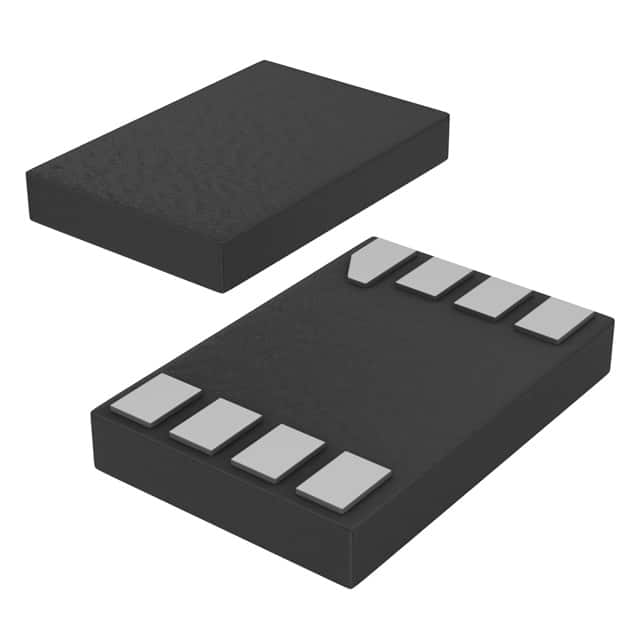
- Package: SOT753 (SC-70)
- Essence: Buffering and level shifting signals in digital circuits
- Packaging/Quantity: Tape and Reel, 3000 pieces per reel
Specifications
- Supply Voltage Range: 0.8V to 3.6V
- High-Level Input Voltage: 0.7 x VCC
- Low-Level Input Voltage: 0.3 x VCC
- High-Level Output Voltage: 0.7 x VCC
- Low-Level Output Voltage: 0.1 x VCC
- Maximum Operating Frequency: 200 MHz
- Propagation Delay: 2.5 ns (typical)
Detailed Pin Configuration
The 74AUP1G885GD,125 IC has the following pin configuration:
____
   A -|    |- VCC
   B -|    |- Y
 GND -|____|- NC
Functional Features
- Schmitt-trigger input for hysteresis
- Open-drain output for flexible signal routing
- Wide supply voltage range for compatibility with various systems
- Low power consumption
- High noise immunity
- ESD protection on all pins
Advantages
- Small package size allows for space-saving designs
- Wide supply voltage range enables compatibility with different power sources
- Schmitt-trigger input provides noise immunity and signal conditioning
- Open-drain output allows for easy interfacing with other devices
- Low power consumption makes it suitable for battery-powered applications
Disadvantages
- Limited maximum operating frequency compared to some other logic gates
- Only one gate available in a single package
- Open-drain output requires external pull-up resistor for proper operation
Working Principles
The 74AUP1G885GD,125 is a single Schmitt-trigger buffer with an open-drain output. It operates by amplifying and conditioning digital signals. The Schmitt-trigger input provides hysteresis, ensuring noise immunity and stable output transitions. The open-drain output allows the IC to drive signals to different voltage levels by connecting an external pull-up resistor.
Detailed Application Field Plans
The 74AUP1G885GD,125 can be used in various applications, including: - Level shifting in mixed-voltage systems - Signal buffering in communication interfaces - Sensor signal conditioning - General-purpose logic level conversion - Battery-powered devices
Detailed and Complete Alternative Models
Some alternative models that can be considered as alternatives to the 74AUP1G885GD,125 are: - SN74LVC1G07DBVR - MC74VHC1GT50DTT1G - TC7SZU04FU
These alternative models offer similar functionality and characteristics, providing options for different design requirements.
Word count: 314 words
Enumere 10 preguntas y respuestas comunes relacionadas con la aplicación de 74AUP1G885GD,125 en soluciones técnicas
Sure! Here are 10 common questions and answers related to the application of 74AUP1G885GD,125 in technical solutions:
Q1: What is the function of the 74AUP1G885GD,125? A1: The 74AUP1G885GD,125 is a single configurable multiple-function gate that can be used as a buffer, gate, or level shifter.
Q2: What is the operating voltage range of the 74AUP1G885GD,125? A2: The operating voltage range is from 0.8V to 3.6V.
Q3: Can the 74AUP1G885GD,125 be used in battery-powered applications? A3: Yes, the low operating voltage range makes it suitable for battery-powered applications.
Q4: What is the maximum output current of the 74AUP1G885GD,125? A4: The maximum output current is typically 32mA.
Q5: Can the 74AUP1G885GD,125 be used as a level shifter between different voltage domains? A5: Yes, it can be used as a level shifter between voltage domains with different logic levels.
Q6: Does the 74AUP1G885GD,125 have any input protection features? A6: Yes, it has integrated ESD protection diodes on all inputs.
Q7: What is the propagation delay of the 74AUP1G885GD,125? A7: The typical propagation delay is around 2.5ns.
Q8: Can the 74AUP1G885GD,125 be used in high-speed applications? A8: Yes, it is designed for high-speed operation and can be used in various high-speed applications.
Q9: Is the 74AUP1G885GD,125 compatible with other logic families? A9: Yes, it is compatible with a wide range of logic families, including CMOS and TTL.
Q10: What package options are available for the 74AUP1G885GD,125? A10: The 74AUP1G885GD,125 is available in various package options, such as SOT353 and XSON6.