

Consulte las especificaciones para obtener detalles del producto.
74AUP2G241DC,125
Basic Information Overview
- Category: Integrated Circuit (IC)
- Use: Logic Gate
- Characteristics: Dual Buffer/Line Driver
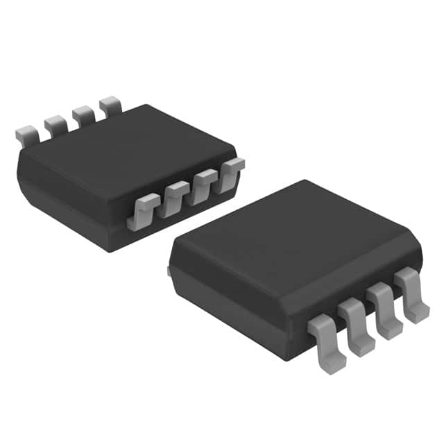
- Package: SOT353 (SC-88A)
- Essence: High-speed CMOS technology
- Packaging/Quantity: Tape and Reel, 3000 pieces per reel
Specifications
- Supply Voltage Range: 0.8V to 3.6V
- Input Voltage Range: -0.5V to VCC + 0.5V
- Output Voltage Range: 0V to VCC
- Operating Temperature Range: -40°C to +85°C
- Propagation Delay: 1.9ns (typical)
- Output Drive Capability: ±24mA
Detailed Pin Configuration
The 74AUP2G241DC,125 IC has the following pin configuration:
___________
  IN1 --|           |-- OUT1
  IN2 --|           |-- OUT2
  GND --|           |-- VCC
        |___________|
Functional Features
- Dual buffer/line driver with independent input and output pins.
- High-speed operation due to advanced CMOS technology.
- Low power consumption.
- Wide supply voltage range allows compatibility with various systems.
- Schmitt-trigger inputs for improved noise immunity.
Advantages
- Compact package size enables space-saving designs.
- High-speed performance suitable for applications requiring quick signal transmission.
- Low power consumption helps in energy-efficient designs.
- Wide supply voltage range enhances compatibility with different systems.
- Schmitt-trigger inputs provide better noise immunity.
Disadvantages
- Limited output drive capability may not be suitable for high-current applications.
- Operating temperature range may restrict usage in extreme environments.
- Availability of alternative models with additional features may limit its adoption in certain applications.
Working Principles
The 74AUP2G241DC,125 is a dual buffer/line driver IC that operates on high-speed CMOS technology. It receives input signals from IN1 and IN2 pins and provides buffered output signals at OUT1 and OUT2 pins. The advanced CMOS technology ensures fast signal propagation with low power consumption. The Schmitt-trigger inputs improve noise immunity by providing hysteresis to the input signals.
Detailed Application Field Plans
The 74AUP2G241DC,125 IC finds applications in various fields, including: - Communication systems - Data transmission - Industrial automation - Consumer electronics - Automotive electronics
Detailed and Complete Alternative Models
Some alternative models that can be considered as alternatives to the 74AUP2G241DC,125 IC are: - 74AUP2G07DC,125: Dual Buffer/Inverter - 74AUP2G126DC,125: Dual Bus Buffer Gate - 74AUP2G240DC,125: Dual Inverting Buffer/Line Driver
These alternative models offer similar functionality but may have additional features or different package options.
Word count: 278 words
Enumere 10 preguntas y respuestas comunes relacionadas con la aplicación de 74AUP2G241DC,125 en soluciones técnicas
Sure! Here are 10 common questions and answers related to the application of 74AUP2G241DC,125 in technical solutions:
1. What is the function of the 74AUP2G241DC,125? The 74AUP2G241DC,125 is a dual buffer/line driver IC that can be used to amplify and buffer digital signals.
2. What is the operating voltage range of the 74AUP2G241DC,125? The operating voltage range of the 74AUP2G241DC,125 is typically between 0.8V and 3.6V.
3. Can the 74AUP2G241DC,125 be used with both CMOS and TTL logic levels? Yes, the 74AUP2G241DC,125 is compatible with both CMOS and TTL logic levels.
4. What is the maximum output current of the 74AUP2G241DC,125? The maximum output current of the 74AUP2G241DC,125 is typically around 32mA.
5. Is the 74AUP2G241DC,125 suitable for high-speed applications? Yes, the 74AUP2G241DC,125 is designed for high-speed operation and can be used in applications with fast switching speeds.
6. Can the 74AUP2G241DC,125 be used as a level shifter? Yes, the 74AUP2G241DC,125 can be used as a level shifter to convert signals between different voltage levels.
7. Does the 74AUP2G241DC,125 have built-in protection features? Yes, the 74AUP2G241DC,125 has built-in ESD protection diodes to safeguard against electrostatic discharge.
8. What is the package type of the 74AUP2G241DC,125? The 74AUP2G241DC,125 is available in a small SOT353 package.
9. Can the 74AUP2G241DC,125 be used in battery-powered applications? Yes, the 74AUP2G241DC,125 has a low power consumption and can be used in battery-powered applications.
10. Are there any recommended application circuits for the 74AUP2G241DC,125? Yes, the datasheet of the 74AUP2G241DC,125 provides several recommended application circuits that can be used as reference designs.
Please note that the answers provided here are general and may vary depending on specific design requirements and conditions. It is always recommended to refer to the datasheet and consult with technical experts for accurate information and guidance.