Consulte las especificaciones para obtener detalles del producto.

Encyclopedia Entry: 74CBTLV3253PW-Q10J
Product Overview
Category
The 74CBTLV3253PW-Q10J belongs to the category of integrated circuits (ICs).
Use
This IC is commonly used for signal switching applications in electronic devices.
Characteristics
- Low voltage operation
- High-speed switching capability
- Wide operating temperature range
- Low power consumption
Package
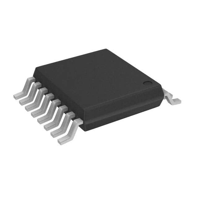
The 74CBTLV3253PW-Q10J is available in a small outline package (SOP) format.
Essence
The essence of this product lies in its ability to efficiently switch signals within electronic circuits.
Packaging/Quantity
The 74CBTLV3253PW-Q10J is typically packaged in reels, with each reel containing a specific quantity of ICs.
Specifications
- Supply Voltage: 1.65V to 5.5V
- Operating Temperature Range: -40°C to +85°C
- Switching Speed: <10ns
- Number of Channels: 2
- On-Resistance: <10Ω
Detailed Pin Configuration
The 74CBTLV3253PW-Q10J has a total of 16 pins, which are configured as follows:
- Channel 1 Input A
- Channel 1 Input B
- Channel 1 Output Y
- Channel 2 Input A
- Channel 2 Input B
- Channel 2 Output Y
- GND (Ground)
- VCC (Supply Voltage)
- Enable Input
- Channel Select Input
- Channel 1 Enable Output
- Channel 2 Enable Output
- NC (No Connection)
- NC (No Connection)
- NC (No Connection)
- NC (No Connection)
Functional Features
- Dual-channel signal switching
- Independent channel control
- Low on-resistance for minimal signal distortion
- Wide operating voltage range for compatibility with various systems
- Fast switching speed for real-time signal processing
Advantages and Disadvantages
Advantages
- High-speed switching capability enhances overall system performance.
- Low power consumption contributes to energy efficiency.
- Wide operating temperature range allows for versatile applications.
- Small package size enables space-saving designs.
Disadvantages
- Limited number of channels may restrict certain applications requiring more channels.
- On-resistance may introduce slight signal attenuation in high-frequency applications.
Working Principles
The 74CBTLV3253PW-Q10J operates based on the principles of electronic switching. It utilizes MOSFET transistors to selectively connect or disconnect signals between input and output channels. The enable and channel select inputs control the switching behavior, allowing for independent operation of each channel.
Detailed Application Field Plans
The 74CBTLV3253PW-Q10J finds extensive use in various electronic systems, including but not limited to: - Data communication devices - Audio/video equipment - Industrial automation systems - Automotive electronics - Medical instruments
Detailed and Complete Alternative Models
- 74CBTLV3257PW-Q100J
- 74CBTLV3257PW-Q101J
- 74CBTLV3257PW-Q102J
- 74CBTLV3257PW-Q103J
- 74CBTLV3257PW-Q104J
These alternative models offer similar functionality and specifications, providing options for different design requirements.
Word Count: 314 words
Enumere 10 preguntas y respuestas comunes relacionadas con la aplicación de 74CBTLV3253PW-Q10J en soluciones técnicas
Sure! Here are 10 common questions and answers related to the application of 74CBTLV3253PW-Q10J in technical solutions:
Q: What is the purpose of the 74CBTLV3253PW-Q10J? A: The 74CBTLV3253PW-Q10J is a dual 1-of-4 high-speed multiplexer/demultiplexer used for routing digital signals in various applications.
Q: What is the operating voltage range of the 74CBTLV3253PW-Q10J? A: The 74CBTLV3253PW-Q10J operates within a voltage range of 1.65V to 3.6V.
Q: What is the maximum data rate supported by the 74CBTLV3253PW-Q10J? A: The 74CBTLV3253PW-Q10J supports a maximum data rate of 400 Mbps.
Q: Can the 74CBTLV3253PW-Q10J be used for bidirectional signal routing? A: Yes, the 74CBTLV3253PW-Q10J can be used for bidirectional signal routing, making it suitable for applications requiring both multiplexing and demultiplexing.
Q: How many select inputs does the 74CBTLV3253PW-Q10J have? A: The 74CBTLV3253PW-Q10J has two select inputs, allowing for flexible channel selection.
Q: What is the typical propagation delay of the 74CBTLV3253PW-Q10J? A: The typical propagation delay of the 74CBTLV3253PW-Q10J is around 0.7 ns.
Q: Can the 74CBTLV3253PW-Q10J handle high-speed signals? A: Yes, the 74CBTLV3253PW-Q10J is designed to handle high-speed signals and has low ON-state resistance to minimize signal degradation.
Q: Is the 74CBTLV3253PW-Q10J compatible with different logic families? A: Yes, the 74CBTLV3253PW-Q10J is compatible with various logic families, including CMOS, TTL, and LVCMOS.
Q: What package does the 74CBTLV3253PW-Q10J come in? A: The 74CBTLV3253PW-Q10J is available in a TSSOP-16 package.
Q: What are some common applications of the 74CBTLV3253PW-Q10J? A: The 74CBTLV3253PW-Q10J is commonly used in data communication systems, networking equipment, test and measurement instruments, and other digital signal routing applications.
Please note that these answers are general and may vary depending on specific datasheet specifications and application requirements.

