

Consulte las especificaciones para obtener detalles del producto.
74HC3G07DC,125
Basic Information Overview
- Category: Integrated Circuit (IC)
- Use: Logic Gate Buffer/Driver
- Characteristics: Triple Buffer/Driver with Open-Drain Outputs
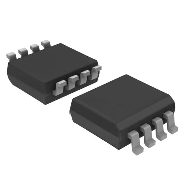
- Package: SOT353 (SC-88A)
- Essence: High-Speed CMOS Technology
- Packaging/Quantity: Tape and Reel, 3000 pieces per reel
Specifications
- Supply Voltage Range: 2.0V to 6.0V
- Input Voltage Range: GND to VCC
- Output Voltage Range: GND to VCC
- Maximum Operating Frequency: 80 MHz
- Propagation Delay: 5 ns (typical)
- Output Current: ±8 mA
- Operating Temperature Range: -40°C to +125°C
Detailed Pin Configuration
The 74HC3G07DC,125 has a total of six pins: 1. GND: Ground reference for the IC. 2. A: Input pin for the first buffer/driver. 3. B: Input pin for the second buffer/driver. 4. C: Input pin for the third buffer/driver. 5. Y: Output pin for all three buffer/drivers. 6. VCC: Positive supply voltage input.
Functional Features
- Triple Buffer/Driver: The IC contains three independent buffer/drivers, allowing it to drive multiple loads simultaneously.
- Open-Drain Outputs: The outputs are open-drain, which means they can be connected directly to other devices or pulled up using external resistors.
- High-Speed Operation: Utilizes high-speed CMOS technology, enabling fast switching times and high-frequency operation.
- Wide Voltage Range: Supports a wide supply voltage range, making it compatible with various digital systems.
- Low Power Consumption: Consumes low power, making it suitable for battery-powered applications.
Advantages and Disadvantages
Advantages: - Versatile: Can be used in a wide range of digital applications. - Compact Size: The SOT353 package offers a small footprint, saving board space. - High-Speed Operation: Enables efficient data transmission in high-frequency systems.
Disadvantages: - Limited Output Current: The maximum output current of ±8 mA may not be sufficient for driving heavy loads. - Lack of ESD Protection: The IC does not provide built-in electrostatic discharge (ESD) protection, requiring external measures to prevent damage from static electricity.
Working Principles
The 74HC3G07DC,125 operates as a buffer/driver by amplifying and shaping digital signals. It takes input signals from pins A, B, and C and provides corresponding amplified outputs at pin Y. The open-drain outputs allow easy interfacing with other devices or circuits. The IC's high-speed CMOS technology ensures fast switching times and reliable operation.
Detailed Application Field Plans
The 74HC3G07DC,125 finds applications in various digital systems, including but not limited to: 1. Communication Systems: Used for signal buffering and level shifting in communication interfaces such as UART, SPI, and I2C. 2. Microcontroller Interfacing: Enables connection between microcontrollers and peripheral devices, such as sensors, displays, and memory modules. 3. Industrial Control Systems: Provides signal conditioning and driving capabilities in industrial automation and control systems. 4. Automotive Electronics: Used for signal buffering and level translation in automotive electronics, including infotainment systems and body control modules.
Detailed and Complete Alternative Models
Some alternative models that offer similar functionality to the 74HC3G07DC,125 are: - SN74LVC3G07: Triple Buffer/Driver with Open-Drain Outputs, available in different package options. - MC74VHC1G07: Single Buffer/Driver with Open-Drain Output, suitable for low-power applications. - 74AHC3G07: Triple Buffer/Driver with Push-Pull Outputs, offering higher output current capability.
Note: The above alternatives may have different specifications and pin configurations. It is recommended to refer to their respective datasheets for detailed information.
Word count: 527 words
Enumere 10 preguntas y respuestas comunes relacionadas con la aplicación de 74HC3G07DC,125 en soluciones técnicas
Sure! Here are 10 common questions and answers related to the application of 74HC3G07DC,125 in technical solutions:
Q: What is the function of the 74HC3G07DC,125? A: The 74HC3G07DC,125 is a triple buffer with open-drain output that can be used for voltage level translation and signal buffering.
Q: What is the operating voltage range of the 74HC3G07DC,125? A: The 74HC3G07DC,125 operates within a voltage range of 2V to 6V.
Q: Can the 74HC3G07DC,125 handle bidirectional communication? A: No, the 74HC3G07DC,125 is unidirectional and can only be used for one-way signal transmission.
Q: What is the maximum data rate supported by the 74HC3G07DC,125? A: The 74HC3G07DC,125 can support data rates up to 100 MHz.
Q: How many buffers are there in the 74HC3G07DC,125? A: The 74HC3G07DC,125 has three independent buffers.
Q: Can the 74HC3G07DC,125 be used for level shifting between different voltage domains? A: Yes, the 74HC3G07DC,125 can be used for level shifting between different voltage domains, as long as the voltage levels are within its operating range.
Q: What is the output current capability of the 74HC3G07DC,125? A: The 74HC3G07DC,125 has a typical output current capability of 8 mA.
Q: Is the 74HC3G07DC,125 compatible with both CMOS and TTL logic levels? A: Yes, the 74HC3G07DC,125 is compatible with both CMOS and TTL logic levels.
Q: Can the 74HC3G07DC,125 be used in high-speed applications? A: Yes, the 74HC3G07DC,125 can be used in high-speed applications due to its fast propagation delay and transition times.
Q: What is the package type of the 74HC3G07DC,125? A: The 74HC3G07DC,125 is available in a small SOT353 package.
Please note that these answers are general and may vary depending on the specific datasheet and application requirements.