

Consulte las especificaciones para obtener detalles del producto.
74LVC8T245BQ-Q100J
Basic Information Overview
- Category: Integrated Circuit (IC)
- Use: Level Shifting and Signal Buffering
- Characteristics: Low Voltage CMOS Octal Bus Transceiver with 5V Tolerant Inputs/Outputs
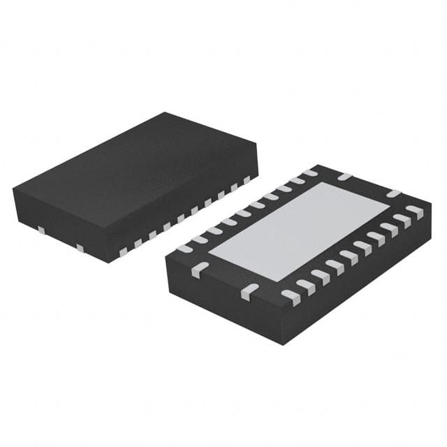
- Package: 48-pin Very Thin Quad Flat No-Lead (VQFN)
- Essence: This IC is designed to provide level shifting and signal buffering capabilities for various digital systems.
- Packaging/Quantity: Available in tape and reel packaging, with a quantity of 2500 units per reel.
Specifications
- Supply Voltage Range: 1.65V to 3.6V
- High-Level Input Voltage: 2V to VCC + 0.3V
- Low-Level Input Voltage: -0.3V to 0.8V
- High-Level Output Voltage: VCC - 0.3V
- Low-Level Output Voltage: 0.3V
- Maximum Operating Frequency: 400 MHz
- Propagation Delay: 4.3 ns (Max)
Detailed Pin Configuration
The 74LVC8T245BQ-Q100J has a total of 48 pins, which are arranged as follows:
- OE (Output Enable) 1
- A1 (Data Input/Output) 1
- B1 (Data Input/Output) 1
- GND (Ground)
- B2 (Data Input/Output) 2
- A2 (Data Input/Output) 2
- VCC (Supply Voltage)
- DIR (Direction Control)
- OE (Output Enable) 2
- B3 (Data Input/Output) 3
- A3 (Data Input/Output) 3
- GND (Ground)
- A4 (Data Input/Output) 4
- B4 (Data Input/Output) 4
- VCC (Supply Voltage)
- DIR (Direction Control)
- OE (Output Enable) 3
- B5 (Data Input/Output) 5
- A5 (Data Input/Output) 5
- GND (Ground)
- B6 (Data Input/Output) 6
- A6 (Data Input/Output) 6
- VCC (Supply Voltage)
- DIR (Direction Control)
- OE (Output Enable) 4
- B7 (Data Input/Output) 7
- A7 (Data Input/Output) 7
- GND (Ground)
- A8 (Data Input/Output) 8
- B8 (Data Input/Output) 8
- VCC (Supply Voltage)
- DIR (Direction Control)
- GND (Ground)
- B9 (Data Input/Output) 9
- A9 (Data Input/Output) 9
- VCC (Supply Voltage)
- DIR (Direction Control)
- GND (Ground)
- B10 (Data Input/Output) 10
- A10 (Data Input/Output) 10
- VCC (Supply Voltage)
- DIR (Direction Control)
- GND (Ground)
- B11 (Data Input/Output) 11
- A11 (Data Input/Output) 11
- VCC (Supply Voltage)
- DIR (Direction Control)
- GND (Ground)
Functional Features
- Bidirectional voltage level shifting between 1.8V and 5V systems.
- 5V tolerant inputs and outputs for interfacing with higher voltage systems.
- Automatic direction control based on DIR pin input.
- Output enable (OE) pins to disable the outputs when not in use.
Advantages
- Wide supply voltage range allows compatibility with various digital systems.
- High-speed operation with a maximum frequency of 400 MHz.
- Low propagation delay ensures efficient signal transmission.
- 5V tolerant inputs/outputs provide flexibility in system integration.
Disadvantages
- Limited number of data input/output channels (8 channels).
- May require additional external components for specific applications.
Working Principles
The 74LVC8T245BQ-Q100J is an octal bus transceiver that facilitates bidirectional level shifting between 1.8V and 5V systems. It operates by automatically controlling the direction of data flow based on the input provided to the DIR pin. The output enable (OE) pins allow the user to disable the outputs when not required, reducing power consumption.
Detailed Application Field Plans
The 74LVC8T245BQ-Q100J is commonly used in various applications,
Enumere 10 preguntas y respuestas comunes relacionadas con la aplicación de 74LVC8T245BQ-Q100J en soluciones técnicas
Sure! Here are 10 common questions and answers related to the application of 74LVC8T245BQ-Q100J in technical solutions:
Question: What is the function of the 74LVC8T245BQ-Q100J?
Answer: The 74LVC8T245BQ-Q100J is an octal bus transceiver with 3-state outputs, used for bidirectional level shifting between different voltage domains.Question: What is the operating voltage range of the 74LVC8T245BQ-Q100J?
Answer: The 74LVC8T245BQ-Q100J operates within a voltage range of 1.65V to 5.5V.Question: How many channels does the 74LVC8T245BQ-Q100J have?
Answer: The 74LVC8T245BQ-Q100J has 8 bidirectional channels.Question: Can the 74LVC8T245BQ-Q100J handle high-speed data transmission?
Answer: Yes, the 74LVC8T245BQ-Q100J is designed for high-speed operation and can support data rates up to 400 Mbps.Question: Is the 74LVC8T245BQ-Q100J compatible with both TTL and CMOS logic levels?
Answer: Yes, the 74LVC8T245BQ-Q100J is compatible with both TTL and CMOS logic levels, making it versatile for various applications.Question: Does the 74LVC8T245BQ-Q100J have built-in ESD protection?
Answer: Yes, the 74LVC8T245BQ-Q100J has built-in ESD protection, ensuring robustness against electrostatic discharge.Question: Can the 74LVC8T245BQ-Q100J be used for level shifting between different voltage domains?
Answer: Yes, the 74LVC8T245BQ-Q100J is commonly used for bidirectional level shifting between voltage domains, making it useful in mixed-voltage systems.Question: What is the maximum output current of the 74LVC8T245BQ-Q100J?
Answer: The 74LVC8T245BQ-Q100J can source or sink up to 32 mA per channel.Question: Does the 74LVC8T245BQ-Q100J have internal pull-up or pull-down resistors?
Answer: No, the 74LVC8T245BQ-Q100J does not have internal pull-up or pull-down resistors. External resistors may be required for specific applications.Question: Is the 74LVC8T245BQ-Q100J available in a lead-free package?
Answer: Yes, the 74LVC8T245BQ-Q100J is available in a lead-free package, complying with RoHS requirements.
Please note that these answers are general and may vary depending on the specific datasheet and application requirements.