

Consulte las especificaciones para obtener detalles del producto.
PDTA113ET,215
Product Category: Transistor
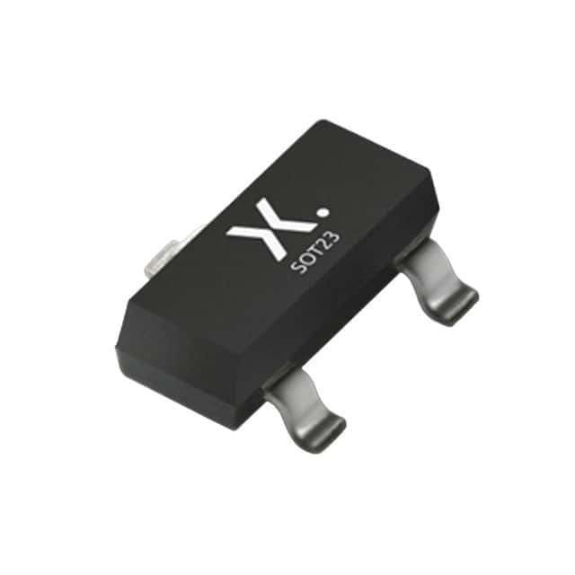
Basic Information Overview: - Category: NPN Bipolar Transistor - Use: Amplification and Switching - Characteristics: High voltage, low current, small package size - Package: SOT416 (SC-75) - Essence: Small signal transistor for general purpose applications - Packaging/Quantity: Tape and Reel, 3000 units per reel
Specifications: - Collector-Base Voltage (VCBO): 50V - Collector-Emitter Voltage (VCEO): 50V - Emitter-Base Voltage (VEBO): 5V - Collector Current (IC): 100mA - Total Power Dissipation (PTOT): 250mW - Transition Frequency (fT): 200MHz - Operating Temperature Range (Tj): -55°C to +150°C
Detailed Pin Configuration: - Pin 1 (Emitter) - Pin 2 (Base) - Pin 3 (Collector)
Functional Features: - High voltage capability - Low leakage current - Fast switching speed - Small package size
Advantages: - Suitable for high voltage applications - Compact and space-saving design - Wide operating temperature range
Disadvantages: - Limited collector current compared to some alternatives - Sensitive to static electricity due to small package size
Working Principles: The PDTA113ET,215 operates based on the principles of bipolar junction transistors, utilizing the flow of charge carriers to amplify or switch electronic signals.
Detailed Application Field Plans: - Audio amplification circuits - Signal processing circuits - Switching circuits in portable devices
Detailed and Complete Alternative Models: - BC847B,215 - MMBT3904LT1G - 2N3904
This comprehensive entry provides a detailed overview of the PDTA113ET,215, covering its category, basic information, specifications, pin configuration, functional features, advantages and disadvantages, working principles, application field plans, and alternative models.
Enumere 10 preguntas y respuestas comunes relacionadas con la aplicación de PDTA113ET,215 en soluciones técnicas
What is PDTA113ET,215?
- PDTA113ET,215 is a NPN resistor-equipped transistor designed for use in general-purpose amplifier and switching applications.
What are the key features of PDTA113ET,215?
- The key features of PDTA113ET,215 include its high current gain, low collector-emitter saturation voltage, and built-in resistor for biasing.
What are the typical applications of PDTA113ET,215?
- Typical applications of PDTA113ET,215 include audio amplification, signal processing, and general switching circuits.
What is the maximum collector current of PDTA113ET,215?
- The maximum collector current of PDTA113ET,215 is 100mA.
What is the maximum power dissipation of PDTA113ET,215?
- The maximum power dissipation of PDTA113ET,215 is 200mW.
What is the voltage rating for PDTA113ET,215?
- The voltage rating for PDTA113ET,215 is 50V.
What is the thermal resistance of PDTA113ET,215?
- The thermal resistance of PDTA113ET,215 is typically 625°C/W.
What are the recommended operating conditions for PDTA113ET,215?
- The recommended operating conditions for PDTA113ET,215 include a collector current of 10mA to 100mA and a collector-emitter voltage of 45V.
Can PDTA113ET,215 be used in high-frequency applications?
- No, PDTA113ET,215 is not suitable for high-frequency applications due to its limited frequency response.
Are there any specific layout considerations when using PDTA113ET,215 in a circuit?
- It is recommended to minimize the length of the connections to PDTA113ET,215 and provide adequate heat sinking if operating at high currents or power levels.