

Consulte las especificaciones para obtener detalles del producto.
Encyclopedia Entry: 74ABT827DB,112
Product Overview
Category
The 74ABT827DB,112 belongs to the category of integrated circuits (ICs) and specifically falls under the family of digital logic devices.
Use
This product is commonly used in electronic systems for various applications that require high-speed data processing and manipulation.
Characteristics
- High-speed operation: The 74ABT827DB,112 is designed to operate at high clock frequencies, making it suitable for time-critical applications.
- Low power consumption: This IC is optimized for low power consumption, ensuring efficient energy usage in electronic systems.
- Wide voltage range: It can operate within a wide voltage range, allowing compatibility with different power supply levels.
- Noise immunity: The 74ABT827DB,112 has built-in noise immunity features, enabling reliable operation in noisy environments.
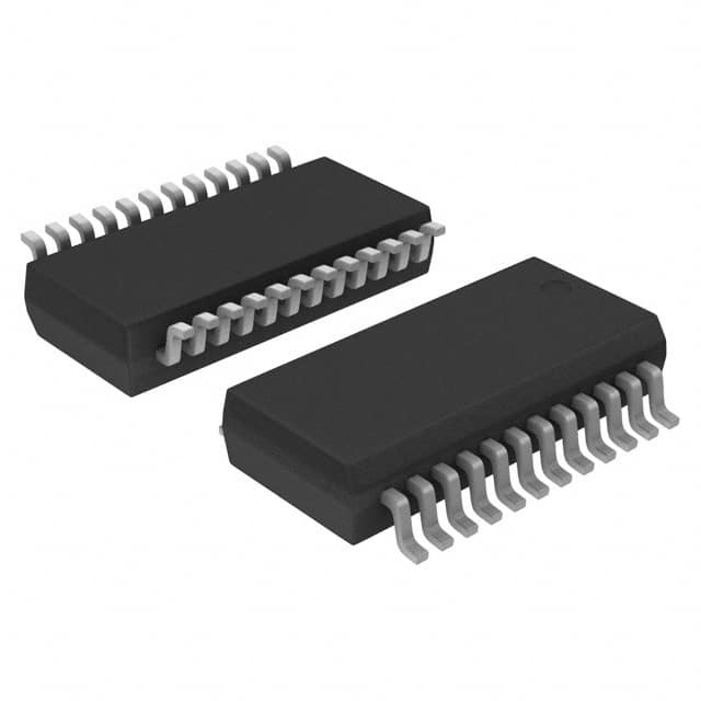
Package and Quantity
The 74ABT827DB,112 is available in a standard dual in-line package (DIP) or surface mount package (SMD). The package contains a single IC.
Specifications
- Logic Family: ABT
- Number of Inputs: 10
- Number of Outputs: 10
- Supply Voltage Range: 4.5V to 5.5V
- Operating Temperature Range: -40°C to +85°C
- Propagation Delay: <10 ns
Pin Configuration
The 74ABT827DB,112 has a total of 20 pins, which are arranged as follows:
Pin 1: Input A0
Pin 2: Input A1
Pin 3: Input A2
Pin 4: Input A3
Pin 5: Input A4
Pin 6: Output Y4
Pin 7: Output Y3
Pin 8: Output Y2
Pin 9: Output Y1
Pin 10: Output Y0
Pin 11: GND (Ground)
Pin 12: Output Enable (OE)
Pin 13: Input B0
Pin 14: Input B1
Pin 15: Input B2
Pin 16: Input B3
Pin 17: Input B4
Pin 18: VCC (Power Supply)
Pin 19: Input Enable (IE)
Pin 20: NC (No Connection)
Functional Features
- Data Multiplexing: The 74ABT827DB,112 can multiplex two sets of data inputs (A and B) onto a single set of outputs (Y).
- Output Enable Control: The OE pin allows the user to enable or disable the outputs, providing flexibility in system design.
- Input Enable Control: The IE pin enables or disables the input buffers, allowing selective data input.
Advantages and Disadvantages
Advantages
- High-speed operation enables efficient data processing.
- Low power consumption contributes to energy efficiency.
- Wide voltage range ensures compatibility with various power supply levels.
- Noise immunity enhances reliability in noisy environments.
Disadvantages
- Limited number of inputs and outputs may restrict certain complex applications.
- Requires external components for complete functionality in a larger system.
Working Principles
The 74ABT827DB,112 operates based on digital logic principles. It utilizes internal circuitry to multiplex and control data inputs and outputs. The IC's high-speed operation is achieved through optimized transistor configurations and signal propagation techniques.
Application Field Plans
The 74ABT827DB,112 finds application in various fields, including: 1. Telecommunications: Used in high-speed data transmission systems. 2. Computer Systems: Employed in data buses and memory interfaces. 3. Industrial Automation: Integrated into control systems for efficient data manipulation. 4. Automotive Electronics: Utilized in automotive communication networks.
Alternative Models
Several alternative models with similar functionality to the 74ABT827DB,112 include: - 74HC827: A CMOS logic IC with comparable characteristics. - SN74LS827: A TTL logic IC offering similar features. - CD54/74AC827: An advanced CMOS IC with improved performance.
These alternative models can be considered based on specific application requirements and compatibility with existing systems.
In conclusion, the 74ABT827DB,112 is a high-speed digital logic IC that offers efficient data multiplexing capabilities. Its low power consumption, wide voltage range, and noise immunity make it suitable for various applications in telecommunications, computer systems, industrial automation, and automotive electronics. While it has limitations in terms of input/output count, it provides advantages in terms of speed and energy efficiency. Several alternative models are available for consideration based on specific needs.
Enumere 10 preguntas y respuestas comunes relacionadas con la aplicación de 74ABT827DB,112 en soluciones técnicas
Sure! Here are 10 common questions and answers related to the application of 74ABT827DB,112 in technical solutions:
Q: What is the function of the 74ABT827DB,112? A: The 74ABT827DB,112 is a 10-bit buffer/driver with 3-state outputs.
Q: What is the maximum operating voltage for the 74ABT827DB,112? A: The maximum operating voltage is 5.5V.
Q: How many 3-state outputs does the 74ABT827DB,112 have? A: It has 10 3-state outputs.
Q: What is the output current capability of the 74ABT827DB,112? A: The output current capability is typically 32mA.
Q: Can the 74ABT827DB,112 be used as a level shifter? A: Yes, it can be used as a level shifter between different voltage domains.
Q: What is the propagation delay of the 74ABT827DB,112? A: The propagation delay is typically 3.5ns.
Q: Is the 74ABT827DB,112 compatible with TTL logic levels? A: Yes, it is compatible with both TTL and CMOS logic levels.
Q: Can the 74ABT827DB,112 be used in high-speed applications? A: Yes, it is designed for high-speed operation and can be used in such applications.
Q: Does the 74ABT827DB,112 have built-in protection against electrostatic discharge (ESD)? A: Yes, it has ESD protection on all inputs and outputs.
Q: Can the 74ABT827DB,112 be used in automotive applications? A: Yes, it is qualified for automotive applications and meets relevant industry standards.
Please note that the answers provided here are general and may vary depending on the specific datasheet and application requirements.