

Consulte las especificaciones para obtener detalles del producto.
N74F543DB,112
Product Overview
- Category: Integrated Circuit (IC)
- Use: Digital Logic
- Characteristics: High-speed, Octal D-type flip-flop with 3-state outputs
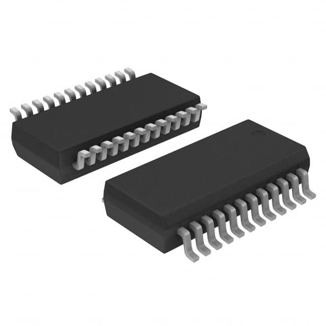
- Package: SOIC (Small Outline Integrated Circuit)
- Essence: Flip-flop with multiple outputs and high-speed operation
- Packaging/Quantity: Tape and Reel, 2500 units per reel
Specifications
- Supply Voltage Range: 4.5V to 5.5V
- Input Voltage Range: 0V to VCC
- Output Voltage Range: 0V to VCC
- Operating Temperature Range: -40°C to +85°C
- Propagation Delay Time: 6 ns (typical)
- Output Current: ±24 mA
Detailed Pin Configuration
The N74F543DB,112 IC has a total of 20 pins. The pin configuration is as follows:
- GND (Ground)
- D0 (Data input 0)
- D1 (Data input 1)
- D2 (Data input 2)
- D3 (Data input 3)
- D4 (Data input 4)
- D5 (Data input 5)
- D6 (Data input 6)
- D7 (Data input 7)
- OE (Output Enable)
- CP (Clock Pulse)
- MR (Master Reset)
- Q0 (Flip-flop output 0)
- Q1 (Flip-flop output 1)
- Q2 (Flip-flop output 2)
- Q3 (Flip-flop output 3)
- Q4 (Flip-flop output 4)
- Q5 (Flip-flop output 5)
- Q6 (Flip-flop output 6)
- VCC (Supply Voltage)
Functional Features
- Octal D-type flip-flop with 3-state outputs
- High-speed operation with a propagation delay time of 6 ns
- Output enable control for tri-state outputs
- Master reset functionality to clear all flip-flops simultaneously
- Wide operating voltage range for flexibility in various applications
Advantages and Disadvantages
Advantages: - High-speed operation allows for efficient data processing - Multiple outputs provide versatility in circuit design - Tri-state outputs enable bus sharing and reduce conflicts - Wide operating voltage range accommodates different power supply configurations
Disadvantages: - Limited number of flip-flop outputs may restrict certain complex designs - Propagation delay time may affect timing-sensitive applications - Requires careful consideration of clock pulse and master reset signals for proper functioning
Working Principles
The N74F543DB,112 is an octal D-type flip-flop with 3-state outputs. It operates based on the positive edge-triggered principle, where the input data is latched into the flip-flops on the rising edge of the clock pulse. The output state can be enabled or disabled using the output enable (OE) pin. When the OE pin is high, the outputs are active, and when it is low, the outputs are in a high-impedance state.
The master reset (MR) pin allows for simultaneous clearing of all flip-flops, setting their outputs to a known state. This feature is useful during initialization or error recovery.
Detailed Application Field Plans
The N74F543DB,112 IC finds applications in various digital logic systems, including but not limited to:
- Data storage and retrieval systems
- Address decoding circuits
- Bus interface units
- Register banks
- Memory modules
- Control units
- Arithmetic logic units (ALUs)
- Microprocessor systems
Detailed and Complete Alternative Models
- SN74F543DBR - Similar octal D-type flip-flop with 3-state outputs from Texas Instruments
- MC74F543DW - Octal D-type flip-flop with 3-state outputs from ON Semiconductor
- CD54/74F543 - Octal D-type flip-flop with 3-state outputs from Fairchild Semiconductor
These alternative models offer similar functionality and can be considered as substitutes for the N74F543DB,112 IC.
Word count: 511 words
Enumere 10 preguntas y respuestas comunes relacionadas con la aplicación de N74F543DB,112 en soluciones técnicas
Sure! Here are 10 common questions and answers related to the application of N74F543DB,112 in technical solutions:
Q: What is N74F543DB,112? A: N74F543DB,112 is a specific integrated circuit (IC) chip used for various technical applications.
Q: What is the function of N74F543DB,112? A: N74F543DB,112 is an octal transceiver with tri-state outputs, which means it can transmit and receive data between different systems or devices.
Q: What voltage levels does N74F543DB,112 support? A: N74F543DB,112 supports a wide range of voltage levels, typically ranging from 2V to 6V.
Q: How many channels does N74F543DB,112 have? A: N74F543DB,112 has 8 channels, allowing it to handle multiple data transmission simultaneously.
Q: Can N74F543DB,112 be used in both digital and analog applications? A: No, N74F543DB,112 is primarily designed for digital applications and may not be suitable for analog use.
Q: What is the maximum data transfer rate supported by N74F543DB,112? A: The maximum data transfer rate of N74F543DB,112 is typically around 25 MHz.
Q: Does N74F543DB,112 have built-in protection features? A: Yes, N74F543DB,112 includes built-in protection against electrostatic discharge (ESD) and excessive current.
Q: Can N74F543DB,112 be used in high-temperature environments? A: Yes, N74F543DB,112 is designed to operate in a wide temperature range, typically from -40°C to 85°C.
Q: What is the power supply requirement for N74F543DB,112? A: N74F543DB,112 requires a power supply voltage of typically 5V, but it can also operate with lower voltages within its specified range.
Q: Are there any specific application notes or reference designs available for N74F543DB,112? A: Yes, the manufacturer of N74F543DB,112 usually provides application notes and reference designs that can help users understand and implement the IC in their technical solutions.
Please note that the answers provided here are general and may vary depending on the specific datasheet and documentation provided by the manufacturer of N74F543DB,112.