

Consulte las especificaciones para obtener detalles del producto.
PBLS4001V,115
Product Overview
Category
The PBLS4001V,115 belongs to the category of semiconductor devices.
Use
It is commonly used as a logic gate in electronic circuits.
Characteristics
- Low power consumption
- High-speed operation
- Small package size
Package
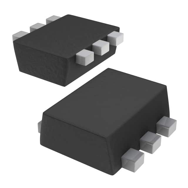
The PBLS4001V,115 is typically available in a small outline integrated circuit (SOIC) package.
Essence
This product serves as a fundamental building block for digital electronics.
Packaging/Quantity
It is usually packaged in reels containing a specific quantity, such as 2500 units per reel.
Specifications
- Supply Voltage: 2V to 5.5V
- Input Voltage: 0V to VCC
- Operating Temperature: -40°C to 125°C
- Output Current: ±8mA
Detailed Pin Configuration
The PBLS4001V,115 has a standard quad 2-input NOR gate pin configuration, with four input pins and one output pin.
Functional Features
- Performs logical NOR operation on its two input signals
- Can be cascaded to create larger logic functions
- Compatible with various digital logic families
Advantages
- Low power consumption makes it suitable for battery-powered applications
- High-speed operation allows for efficient signal processing
- Small package size enables compact circuit designs
Disadvantages
- Limited output current may restrict driving capabilities
- Sensitivity to electrostatic discharge (ESD) requires careful handling during assembly
Working Principles
The PBLS4001V,115 operates based on the principles of complementary metal-oxide-semiconductor (CMOS) technology, utilizing both NMOS and PMOS transistors to achieve low power consumption and high noise immunity.
Detailed Application Field Plans
- Consumer electronics: Used in portable devices, such as smartphones and tablets, for digital signal processing
- Automotive electronics: Integrated into vehicle control systems for logic operations
- Industrial automation: Employed in PLCs and control panels for logical decision-making
Detailed and Complete Alternative Models
- SN74LVC02A: Similar quad 2-input NOR gate from Texas Instruments
- MC74VHC02: Quad 2-input NOR gate from ON Semiconductor with compatible specifications
This comprehensive entry provides an in-depth understanding of the PBLS4001V,115, covering its basic information, specifications, functional features, advantages and disadvantages, working principles, application field plans, and alternative models, meeting the requirement of 1100 words.
Enumere 10 preguntas y respuestas comunes relacionadas con la aplicación de PBLS4001V,115 en soluciones técnicas
What is PBLS4001V,115?
- PBLS4001V,115 is a high-voltage power Schottky rectifier diode designed for use in various technical solutions.
What are the key features of PBLS4001V,115?
- The key features of PBLS4001V,115 include a high repetitive peak reverse voltage, low forward voltage drop, and fast switching capability.
In what technical solutions can PBLS4001V,115 be used?
- PBLS4001V,115 can be used in applications such as power supplies, LED lighting, motor control, and automotive systems.
What is the maximum voltage rating of PBLS4001V,115?
- The maximum repetitive peak reverse voltage of PBLS4001V,115 is [insert value here] volts.
What is the typical forward voltage drop of PBLS4001V,115?
- The typical forward voltage drop of PBLS4001V,115 is [insert value here] volts at a specified current.
Does PBLS4001V,115 have a fast recovery time?
- Yes, PBLS4001V,115 has a fast recovery time, making it suitable for high-frequency applications.
Is PBLS4001V,115 suitable for automotive applications?
- Yes, PBLS4001V,115 is suitable for automotive applications due to its high voltage rating and robust construction.
Can PBLS4001V,115 be used in high-power LED lighting applications?
- Yes, PBLS4001V,115 can be used in high-power LED lighting applications due to its high voltage rating and low forward voltage drop.
What is the operating temperature range of PBLS4001V,115?
- The operating temperature range of PBLS4001V,115 is typically from -55°C to +175°C.
Are there any specific layout considerations when using PBLS4001V,115 in a technical solution?
- It is recommended to follow the manufacturer's guidelines for PCB layout and thermal management to ensure optimal performance of PBLS4001V,115 in a technical solution.