

Consulte las especificaciones para obtener detalles del producto.
TDA8920BTH/N2,118 - English Editing Encyclopedia Entry
Product Overview
Category
TDA8920BTH/N2,118 belongs to the category of audio amplifier integrated circuits.
Use
This product is primarily used for amplifying audio signals in various electronic devices such as audio systems, home theaters, and multimedia speakers.
Characteristics
- High-quality audio amplification
- Efficient power consumption
- Compact size
- Integrated protection features against overvoltage, overcurrent, and thermal issues
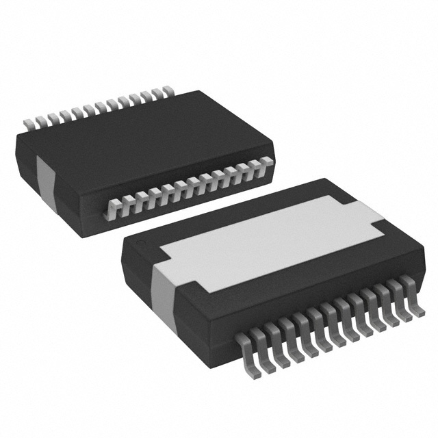
Package
TDA8920BTH/N2,118 is available in a compact surface-mount package, allowing for easy integration into electronic devices.
Essence
The essence of TDA8920BTH/N2,118 lies in its ability to provide high-quality audio amplification while consuming minimal power and offering protection against potential electrical faults.
Packaging/Quantity
This product is typically packaged in reels or tubes, with each reel/tube containing a specific quantity of TDA8920BTH/N2,118 integrated circuits.
Specifications
- Power Supply Voltage: 12V - 36V
- Output Power: Up to 2 x 100W
- Total Harmonic Distortion: <0.1%
- Signal-to-Noise Ratio: >90dB
- Operating Temperature Range: -40°C to +85°C
Detailed Pin Configuration
The TDA8920BTH/N2,118 integrated circuit consists of the following pins:
- VDD: Power supply voltage input
- GND: Ground reference
- INL: Left channel audio input
- INR: Right channel audio input
- STBY: Standby mode control input
- MUTE: Mute control input
- OUTL: Left channel audio output
- OUTR: Right channel audio output
- VSS: Negative power supply voltage input
Functional Features
- High-efficiency Class D amplifier
- Low power consumption in standby mode
- Mute function for audio control
- Overvoltage, overcurrent, and thermal protection
- Short-circuit protection for speaker outputs
Advantages and Disadvantages
Advantages
- High-quality audio amplification with low distortion
- Efficient power consumption, reducing energy costs
- Compact size allows for easy integration into various devices
- Integrated protection features ensure the safety of the amplifier and connected speakers
Disadvantages
- Limited output power compared to some higher-end amplifiers
- Requires an external power supply within the specified voltage range
Working Principles
TDA8920BTH/N2,118 utilizes a Class D amplifier architecture, which employs pulse-width modulation (PWM) techniques to amplify audio signals efficiently. The incoming audio signal is converted into a series of high-frequency pulses, which are then amplified by the power stage of the integrated circuit. These amplified pulses are then filtered and converted back into an analog audio signal, ready to be delivered to the connected speakers.
Detailed Application Field Plans
The TDA8920BTH/N2,118 integrated circuit finds applications in various audio-related fields, including:
- Home audio systems
- Multimedia speakers
- Car audio systems
- Professional audio equipment
- Portable audio devices
Detailed and Complete Alternative Models
- TDA7498E - Similar audio amplifier IC with higher output power capability.
- TAS5611A - Audio amplifier IC with advanced digital signal processing features.
- LM3886 - Popular audio amplifier IC known for its excellent sound quality.
- STA540 - Dual-channel audio amplifier IC suitable for low-power applications.
These alternative models offer different features and specifications, providing options based on specific requirements.
Word count: 515 words
Enumere 10 preguntas y respuestas comunes relacionadas con la aplicación de TDA8920BTH/N2,118 en soluciones técnicas
Question: What is the maximum output power of TDA8920BTH/N2,118?
Answer: The maximum output power of TDA8920BTH/N2,118 is 2x100W.Question: What is the recommended supply voltage range for TDA8920BTH/N2,118?
Answer: The recommended supply voltage range for TDA8920BTH/N2,118 is 18V to 30V.Question: Can TDA8920BTH/N2,118 be used in bridge-tied load (BTL) configuration?
Answer: Yes, TDA8920BTH/N2,118 can be used in bridge-tied load (BTL) configuration.Question: What is the typical efficiency of TDA8920BTH/N2,118?
Answer: The typical efficiency of TDA8920BTH/N2,118 is around 90%.Question: Does TDA8920BTH/N2,118 require external heat sinking?
Answer: Yes, TDA8920BTH/N2,118 requires external heat sinking for proper thermal management.Question: Is TDA8920BTH/N2,118 suitable for automotive applications?
Answer: Yes, TDA8920BTH/N2,118 is suitable for automotive applications.Question: What is the input impedance of TDA8920BTH/N2,118?
Answer: The input impedance of TDA8920BTH/N2,118 is typically 20 kΩ.Question: Can TDA8920BTH/N2,118 operate with a single power supply?
Answer: Yes, TDA8920BTH/N2,118 can operate with a single power supply.Question: What is the standby power consumption of TDA8920BTH/N2,118?
Answer: The standby power consumption of TDA8920BTH/N2,118 is typically less than 0.5W.Question: Are there any specific layout considerations for using TDA8920BTH/N2,118 in a PCB design?
Answer: Yes, it is important to follow the recommended layout guidelines provided in the datasheet for optimal performance of TDA8920BTH/N2,118.