

Consulte las especificaciones para obtener detalles del producto.
TFA9892AUK/N1BZ - English Editing Encyclopedia Entry
Product Overview
Category
TFA9892AUK/N1BZ belongs to the category of audio amplifier integrated circuits.
Use
This product is primarily used for amplifying audio signals in various electronic devices such as smartphones, tablets, and portable media players.
Characteristics
- High-quality audio amplification
- Low power consumption
- Compact size
- Wide input voltage range
- Integrated protection features against overvoltage and short circuits
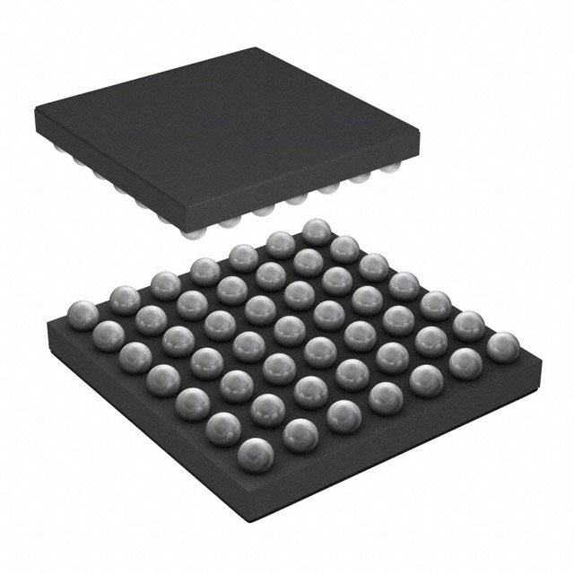
Package
TFA9892AUK/N1BZ is available in a small outline package (SOP) with a specified pin configuration.
Essence
The essence of TFA9892AUK/N1BZ lies in its ability to provide efficient and high-fidelity audio amplification while consuming minimal power.
Packaging/Quantity
This product is typically packaged in reels or tubes, containing a specific quantity per package. Please refer to the manufacturer's documentation for detailed information.
Specifications
- Power Supply Voltage: 2.5V - 5.5V
- Output Power: Up to 3W
- Total Harmonic Distortion + Noise (THD+N): <0.1%
- Signal-to-Noise Ratio (SNR): >90dB
- Operating Temperature Range: -40°C to 85°C
Detailed Pin Configuration
The TFA9892AUK/N1BZ has a total of 16 pins, each serving a specific function. The following table provides a detailed pin configuration:
| Pin Number | Pin Name | Function | |------------|----------|----------| | 1 | VDD | Power supply voltage | | 2 | GND | Ground | | 3 | INL | Left channel audio input | | 4 | INR | Right channel audio input | | 5 | BYP | Bypass capacitor connection | | 6 | VDDA | Analog power supply voltage | | 7 | VSSA | Analog ground | | 8 | OUTL | Left channel audio output | | 9 | OUTR | Right channel audio output | | 10 | SD | Shutdown control input | | 11 | I2CSCL | I2C serial clock input | | 12 | I2CSDA | I2C serial data input/output | | 13 | MUTE | Audio mute control input | | 14 | BST | Boost converter output | | 15 | VDDP | Power supply voltage for boost converter | | 16 | GNDP | Ground for boost converter |
Functional Features
- High-quality audio amplification with low distortion
- Integrated boost converter for efficient power delivery
- Shutdown control for power-saving mode
- I2C interface for easy control and configuration
- Audio mute function for user convenience
Advantages and Disadvantages
Advantages
- Provides high-fidelity audio amplification
- Low power consumption enhances battery life in portable devices
- Compact size allows for integration into small form factor devices
- Integrated protection features ensure device safety
Disadvantages
- May require additional external components for optimal performance
- Limited output power compared to larger audio amplifiers
Working Principles
TFA9892AUK/N1BZ operates by receiving audio signals from the input pins (INL and INR) and amplifying them using an internal amplifier circuit. The amplified audio signals are then delivered to the respective output pins (OUTL and OUTR). The integrated boost converter ensures efficient power delivery, while the shutdown control and audio mute functions provide additional control options.
Detailed Application Field Plans
TFA9892AUK/N1BZ finds applications in various electronic devices, including: - Smartphones - Tablets - Portable media players - Bluetooth speakers - Gaming consoles
Detailed and Complete Alternative Models
- TFA9887HN/N1, TFA9888UK/N1, TFA9890UK/N1 are alternative models that offer similar functionality and features to TFA9892AUK/N1BZ. These models can be considered as alternatives based on specific requirements and design considerations.
In conclusion, TFA9892AUK/N1BZ is a high-quality audio amplifier integrated circuit designed for efficient audio amplification in portable electronic devices. Its compact size, low power consumption, and integrated protection features make it an ideal choice for various applications.
Enumere 10 preguntas y respuestas comunes relacionadas con la aplicación de TFA9892AUK/N1BZ en soluciones técnicas
What is the maximum output power of TFA9892AUK/N1BZ?
- The maximum output power of TFA9892AUK/N1BZ is 3.6W into 8Ω at 5V.Can TFA9892AUK/N1BZ operate with a single supply voltage?
- Yes, TFA9892AUK/N1BZ can operate with a single supply voltage ranging from 2.7V to 5.5V.What is the typical efficiency of TFA9892AUK/N1BZ?
- The typical efficiency of TFA9892AUK/N1BZ is around 90% at 1W output power.Does TFA9892AUK/N1BZ have built-in short-circuit and thermal protection?
- Yes, TFA9892AUK/N1BZ features built-in short-circuit and thermal protection for reliable operation.What is the recommended application circuit for TFA9892AUK/N1BZ?
- The recommended application circuit includes input and output capacitors, as well as appropriate filtering components for optimal performance.Can TFA9892AUK/N1BZ be used in portable audio devices?
- Yes, TFA9892AUK/N1BZ is suitable for use in portable audio devices due to its low power consumption and small footprint.Is TFA9892AUK/N1BZ compatible with common audio input sources?
- Yes, TFA9892AUK/N1BZ is compatible with common audio input sources such as smartphones, tablets, and MP3 players.What is the standby current consumption of TFA9892AUK/N1BZ?
- The standby current consumption of TFA9892AUK/N1BZ is typically less than 1µA, making it suitable for battery-powered applications.Can TFA9892AUK/N1BZ be used in stereo audio systems?
- Yes, TFA9892AUK/N1BZ can be used in stereo audio systems by using two devices for left and right channels.What are the key advantages of using TFA9892AUK/N1BZ in audio amplification applications?
- The key advantages include high efficiency, low power consumption, small package size, and integrated protection features for reliable performance.