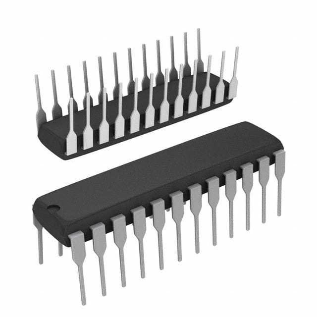
Consulte las especificaciones para obtener detalles del producto.

Encyclopedia Entry: 74F828SPC
Product Information Overview
- Category: Integrated Circuit (IC)
- Use: Digital Logic Function
- Characteristics: High-speed, Low-power consumption
- Package: DIP (Dual In-line Package)
- Essence: 8-bit Buffer/Line Driver
- Packaging/Quantity: Available in tubes of 25 units
Specifications
- Logic Family: 74F
- Number of Inputs: 8
- Number of Outputs: 8
- Supply Voltage: 4.5V to 5.5V
- Operating Temperature Range: -40°C to +85°C
- Propagation Delay: 6 ns (typical)
- Output Current: ±15 mA
Detailed Pin Configuration
The 74F828SPC IC has a total of 20 pins, which are assigned as follows:
- Output 1 (Y1)
- Output 2 (Y2)
- Output 3 (Y3)
- Output 4 (Y4)
- Output 5 (Y5)
- Output 6 (Y6)
- Output 7 (Y7)
- Output 8 (Y8)
- GND (Ground)
- Input 1 (A1)
- Input 2 (A2)
- Input 3 (A3)
- Input 4 (A4)
- Input 5 (A5)
- Input 6 (A6)
- Input 7 (A7)
- Input 8 (A8)
- VCC (Positive Power Supply)
- Enable (EN)
- GND (Ground)
Functional Features
The 74F828SPC is an 8-bit buffer/line driver IC that provides high-speed and low-power consumption digital logic functionality. It is designed to amplify and buffer digital signals, ensuring reliable transmission between different parts of a circuit.
The key functional features of the 74F828SPC include:
- High-speed operation with a typical propagation delay of 6 ns.
- Low power consumption, making it suitable for battery-powered devices.
- Wide operating temperature range (-40°C to +85°C), enabling usage in various environments.
- Output current capability of ±15 mA, allowing it to drive external loads efficiently.
Advantages and Disadvantages
Advantages: - High-speed operation enables quick signal transmission. - Low power consumption prolongs battery life in portable devices. - Wide operating temperature range ensures reliability in extreme conditions. - Output current capability allows driving of external loads without additional amplification.
Disadvantages: - Limited number of inputs and outputs restricts its application in complex circuits. - Availability may be limited due to being an older IC model.
Working Principles
The 74F828SPC operates based on the principles of digital logic. When enabled (EN = HIGH), the inputs (A1-A8) are amplified and buffered, and the corresponding outputs (Y1-Y8) reflect the input logic levels. The IC utilizes internal transistors and gates to achieve this functionality.
Detailed Application Field Plans
The 74F828SPC can be utilized in various applications, including but not limited to:
- Data communication systems
- Microprocessor-based systems
- Industrial control systems
- Automotive electronics
- Consumer electronics
Its ability to amplify and buffer digital signals makes it suitable for any application where reliable signal transmission is required.
Detailed and Complete Alternative Models
If the 74F828SPC is not available or does not meet specific requirements, alternative models with similar functionality can be considered. Some alternatives to the 74F828SPC include:
- 74HC828: High-speed CMOS logic family, compatible with 74F series.
- SN74LS828: Low-power Schottky TTL logic family, compatible with 74F series.
- CD4086: CMOS logic family, 4-bit buffer/line driver.
These alternative models offer similar functionality and can be used as substitutes in various applications.
Word Count: 410 words
Enumere 10 preguntas y respuestas comunes relacionadas con la aplicación de 74F828SPC en soluciones técnicas
Sure! Here are 10 common questions and answers related to the application of 74F828SPC in technical solutions:
Q: What is the 74F828SPC? A: The 74F828SPC is a specific type of integrated circuit (IC) that functions as a bus interface latch.
Q: What is the purpose of the 74F828SPC? A: The 74F828SPC is used to latch data from a bus onto its outputs, allowing for efficient data transfer between different components in a system.
Q: What voltage levels does the 74F828SPC support? A: The 74F828SPC typically supports voltage levels of 5V.
Q: How many bits can the 74F828SPC latch at once? A: The 74F828SPC can latch 8 bits of data simultaneously.
Q: Can the 74F828SPC be used in both synchronous and asynchronous applications? A: Yes, the 74F828SPC can be used in both synchronous and asynchronous applications depending on the system requirements.
Q: What is the maximum clock frequency supported by the 74F828SPC? A: The maximum clock frequency supported by the 74F828SPC is typically around 100 MHz.
Q: Does the 74F828SPC have any built-in error detection or correction mechanisms? A: No, the 74F828SPC does not have any built-in error detection or correction mechanisms. It simply latches the data onto its outputs.
Q: Can the 74F828SPC be cascaded with other ICs to increase the number of latched bits? A: Yes, multiple 74F828SPC ICs can be cascaded together to increase the number of latched bits in a system.
Q: What are some common applications of the 74F828SPC? A: The 74F828SPC is commonly used in data buses, memory systems, and other digital systems where efficient data transfer is required.
Q: Are there any specific precautions or considerations when using the 74F828SPC? A: It is important to ensure that the voltage levels and clock frequencies used in the system are within the specified limits of the 74F828SPC. Additionally, proper decoupling and grounding techniques should be employed for reliable operation.

