Consulte las especificaciones para obtener detalles del producto.

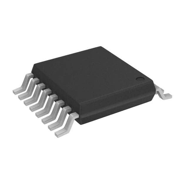
74LCX138MTC
Product Overview
- Category: Integrated Circuit (IC)
- Use: Decoder/Demultiplexer
- Characteristics: Low-voltage, CMOS logic, 3-to-8 line decoder/demultiplexer
- Package: TSSOP (Thin Shrink Small Outline Package)
- Essence: High-performance digital logic device for decoding and demultiplexing applications
- Packaging/Quantity: Tape and Reel, 2500 units per reel
Specifications
- Supply Voltage Range: 1.65V to 3.6V
- Input Voltage Range: 0V to VCC
- Output Voltage Range: 0V to VCC
- Maximum Operating Frequency: 100MHz
- Number of Inputs: 3
- Number of Outputs: 8
- Logic Family: LCX
Detailed Pin Configuration
The 74LCX138MTC has a total of 16 pins. The pin configuration is as follows:
- GND - Ground
- A0 - Address Input 0
- A1 - Address Input 1
- A2 - Address Input 2
- Y0 - Output 0
- Y1 - Output 1
- Y2 - Output 2
- Y3 - Output 3
- Y4 - Output 4
- Y5 - Output 5
- Y6 - Output 6
- Y7 - Output 7
- E1 - Enable Input 1
- E2 - Enable Input 2
- E3 - Enable Input 3
- VCC - Power Supply
Functional Features
- Decodes three binary address inputs into eight mutually exclusive outputs
- Enables easy selection of one output from multiple inputs
- Low-voltage operation allows compatibility with a wide range of systems
- CMOS technology ensures low power consumption and high noise immunity
Advantages and Disadvantages
Advantages: - Wide supply voltage range allows for flexibility in different applications - High-speed operation enables efficient decoding and demultiplexing - Low power consumption makes it suitable for battery-powered devices - Compact TSSOP package saves board space
Disadvantages: - Limited number of inputs may restrict the complexity of address decoding - Not suitable for high-voltage applications due to its low-voltage characteristics
Working Principles
The 74LCX138MTC is based on CMOS technology, which allows for low-voltage operation. It functions as a decoder/demultiplexer by taking three binary address inputs (A0, A1, A2) and generating eight mutually exclusive outputs (Y0-Y7). The enable inputs (E1, E2, E3) control the selection of the output based on the input address.
Detailed Application Field Plans
The 74LCX138MTC can be used in various applications, including but not limited to:
- Address decoding in microcontrollers and microprocessors
- Memory selection in digital systems
- Data routing in communication systems
- Signal demultiplexing in multimedia devices
- Control signal generation in industrial automation
Detailed and Complete Alternative Models
Some alternative models that offer similar functionality to the 74LCX138MTC are:
- 74HC138 - High-speed CMOS logic decoder/demultiplexer
- CD74AC138 - Advanced CMOS decoder/demultiplexer
- SN74LS138 - Low-power Schottky TTL decoder/demultiplexer
These alternatives provide options with different logic families, operating speeds, and power consumption levels, allowing users to choose the most suitable option for their specific requirements.
Word count: 456 words
Enumere 10 preguntas y respuestas comunes relacionadas con la aplicación de 74LCX138MTC en soluciones técnicas
Sure! Here are 10 common questions and answers related to the application of 74LCX138MTC in technical solutions:
Q: What is the 74LCX138MTC? A: The 74LCX138MTC is a 3-to-8 line decoder/demultiplexer integrated circuit (IC) that can be used in digital logic circuits.
Q: What is the purpose of the 74LCX138MTC? A: The purpose of the 74LCX138MTC is to decode a binary input and activate one of the eight output lines based on the input value.
Q: How does the 74LCX138MTC work? A: The IC takes a 3-bit binary input and activates the corresponding output line by decoding the input value using internal logic gates.
Q: What voltage levels does the 74LCX138MTC support? A: The 74LCX138MTC supports voltage levels from 2.0V to 3.6V, making it compatible with both TTL and CMOS logic families.
Q: Can the 74LCX138MTC be cascaded to increase the number of outputs? A: Yes, multiple 74LCX138MTC ICs can be cascaded together to increase the number of outputs beyond eight.
Q: What is the maximum frequency at which the 74LCX138MTC can operate? A: The 74LCX138MTC can operate at a maximum frequency of around 100 MHz.
Q: Can the 74LCX138MTC be used for address decoding in memory systems? A: Yes, the 74LCX138MTC is commonly used for address decoding in memory systems, where it selects the appropriate memory chip based on the address lines.
Q: Does the 74LCX138MTC have any built-in protection features? A: Yes, the IC has built-in ESD (electrostatic discharge) protection to prevent damage from static electricity.
Q: Can the 74LCX138MTC be used in both synchronous and asynchronous applications? A: Yes, the 74LCX138MTC can be used in both synchronous and asynchronous applications depending on the design requirements.
Q: Are there any specific considerations for power supply decoupling when using the 74LCX138MTC? A: Yes, it is recommended to use bypass capacitors near the power supply pins of the IC to ensure stable operation and minimize noise.

