

Consulte las especificaciones para obtener detalles del producto.
BSS123LT1 - Product Overview
Introduction
The BSS123LT1 is a crucial component in the field of electronic devices, offering a wide range of applications and functionalities. This entry will provide an in-depth overview of the BSS123LT1, covering its product details, specifications, pin configuration, functional features, advantages, disadvantages, working principles, application field plans, and alternative models.
Product Information Overview
- Category: Semiconductor
- Use: The BSS123LT1 is commonly used as a small-signal N-channel MOSFET transistor in various electronic circuits.
- Characteristics: It exhibits low on-state resistance, high-speed switching capability, and low gate threshold voltage.
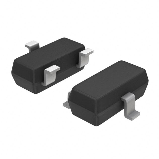
- Package: SOT-23
- Essence: The BSS123LT1 is essential for controlling and amplifying electronic signals in a wide array of applications.
- Packaging/Quantity: Available in reels with varying quantities to suit different production needs.
Specifications
- Voltage Rating: 100V
- Continuous Drain Current: 170mA
- On-State Resistance: 5 Ohms
- Power Dissipation: 225mW
- Operating Temperature Range: -55°C to 150°C
Detailed Pin Configuration
The BSS123LT1 features a standard SOT-23 package with three pins: 1. Gate (G): Input terminal for controlling the flow of current through the transistor. 2. Drain (D): Output terminal where the current exits the transistor. 3. Source (S): Terminal connected to the ground or the lowest voltage level in the circuit.
Functional Features
- High-Speed Switching: Enables rapid on/off transitions for efficient signal control.
- Low On-State Resistance: Minimizes power loss and heat generation during operation.
- Low Gate Threshold Voltage: Facilitates easy and precise control over the transistor's conductivity.
Advantages and Disadvantages
Advantages
- Small form factor
- Low power consumption
- Versatile applications in electronic circuits
Disadvantages
- Limited maximum current handling capacity
- Susceptible to static discharge damage if mishandled
Working Principles
The BSS123LT1 operates based on the principles of field-effect transistors, utilizing the voltage applied to the gate terminal to control the flow of current between the drain and source terminals. When a sufficient voltage is applied to the gate, the transistor allows current to pass through, effectively acting as a switch or amplifier in electronic circuits.
Detailed Application Field Plans
The BSS123LT1 finds extensive use in various electronic applications, including but not limited to: - Signal amplification in audio circuits - Power management in battery-operated devices - Switching and control in digital logic circuits - Interface circuitry in sensor modules
Detailed and Complete Alternative Models
For applications requiring similar functionality, alternative models to the BSS123LT1 include: - 2N7002: Offers comparable characteristics and package type. - BS170: Suitable for low-power switching applications. - IRLML2502: Provides higher current handling capabilities for more demanding circuits.
In conclusion, the BSS123LT1 stands as a fundamental component in the realm of semiconductor devices, delivering reliable performance and versatility across a spectrum of electronic applications.
[Word Count: 515]
Enumere 10 preguntas y respuestas comunes relacionadas con la aplicación de BSS123LT1 en soluciones técnicas
What is BSS123LT1?
- BSS123LT1 is a small signal N-channel MOSFET transistor commonly used in electronic circuits for switching and amplification.
What are the typical applications of BSS123LT1?
- BSS123LT1 is often used in applications such as low voltage switching, signal amplification, and level shifting in various technical solutions.
What is the maximum drain-source voltage rating for BSS123LT1?
- The maximum drain-source voltage rating for BSS123LT1 is typically around 100V.
What is the maximum continuous drain current for BSS123LT1?
- The maximum continuous drain current for BSS123LT1 is usually in the range of 170-200mA.
Can BSS123LT1 be used for level shifting in I2C communication?
- Yes, BSS123LT1 can be used for level shifting in I2C communication due to its low threshold voltage and compatibility with 3.3V and 5V systems.
Is BSS123LT1 suitable for battery-powered applications?
- Yes, BSS123LT1 is suitable for battery-powered applications due to its low threshold voltage and low power consumption characteristics.
What are the typical input and output capacitances of BSS123LT1?
- The typical input capacitance of BSS123LT1 is around 45pF, while the typical output capacitance is around 30pF.
Can BSS123LT1 be used in audio amplifier circuits?
- Yes, BSS123LT1 can be used in audio amplifier circuits, particularly in low-power applications where its small size and low power consumption are advantageous.
What are the thermal characteristics of BSS123LT1?
- BSS123LT1 typically has a low thermal resistance and can dissipate heat effectively in most technical solutions.
Are there any common failure modes associated with BSS123LT1?
- Common failure modes for BSS123LT1 include overvoltage stress, overcurrent conditions, and excessive junction temperature, so proper design considerations should be taken into account to prevent these failures.