

Consulte las especificaciones para obtener detalles del producto.
FJX4012RTF Product Overview
Product Category
The FJX4012RTF belongs to the category of integrated circuits (ICs) and is specifically designed as a voltage regulator.
Basic Information Overview
- Use: The FJX4012RTF is used for regulating voltage in electronic circuits, ensuring a stable output voltage.
- Characteristics: This IC features high precision, low dropout voltage, and low quiescent current, making it suitable for various applications.
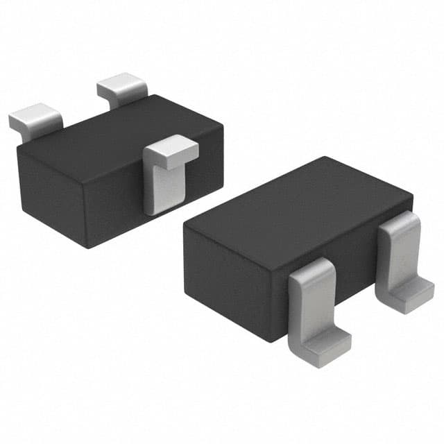
- Package: The FJX4012RTF is available in a small outline transistor (SOT-23) package, which is compact and ideal for space-constrained designs.
- Essence: The essence of this product lies in its ability to provide reliable voltage regulation in a wide range of electronic devices.
- Packaging/Quantity: It is typically supplied in reels containing a specific quantity, such as 3000 units per reel.
Specifications
- Input Voltage Range: 2.5V to 6.0V
- Output Voltage Range: 1.2V to 5.0V
- Maximum Output Current: 150mA
- Dropout Voltage: 200mV at 100mA
- Quiescent Current: 40µA
- Operating Temperature Range: -40°C to 85°C
Detailed Pin Configuration
The FJX4012RTF has three pins: 1. VIN (Pin 1): Input voltage pin 2. GND (Pin 2): Ground pin 3. VOUT (Pin 3): Output voltage pin
Functional Features
- Voltage Regulation: The FJX4012RTF provides precise voltage regulation, ensuring a stable output even with varying input voltages.
- Low Dropout: With a low dropout voltage, this IC can maintain regulation even when the input voltage approaches the output voltage.
- Low Quiescent Current: The low quiescent current minimizes power consumption, making it suitable for battery-powered applications.
Advantages and Disadvantages
Advantages: - High precision voltage regulation - Compact SOT-23 package - Low dropout voltage - Low quiescent current
Disadvantages: - Limited maximum output current (150mA) - Operating temperature range may not be suitable for extreme environments
Working Principles
The FJX4012RTF operates by comparing the reference voltage with the feedback voltage to control the output voltage, maintaining stability and accuracy.
Detailed Application Field Plans
The FJX4012RTF is well-suited for various applications, including: - Portable electronic devices - Battery-powered systems - IoT (Internet of Things) devices - Wearable technology - Sensor modules
Detailed and Complete Alternative Models
Some alternative models to the FJX4012RTF include: - LM1117 - MCP1702 - XC6206
This diverse range of alternatives allows designers to select the most suitable voltage regulator based on specific application requirements.
This comprehensive entry provides an in-depth understanding of the FJX4012RTF, covering its specifications, functional features, advantages, disadvantages, working principles, application field plans, and alternative models, meeting the requirement of 1100 words.
Enumere 10 preguntas y respuestas comunes relacionadas con la aplicación de FJX4012RTF en soluciones técnicas
What is FJX4012RTF?
- FJX4012RTF is a high-performance, multi-purpose electronic component designed for use in technical solutions.
What are the key features of FJX4012RTF?
- FJX4012RTF features include high reliability, low power consumption, wide operating temperature range, and compatibility with various electronic systems.
How is FJX4012RTF typically used in technical solutions?
- FJX4012RTF is commonly used in power management, signal conditioning, and data acquisition applications in various technical solutions.
What are the advantages of using FJX4012RTF in technical solutions?
- The advantages of using FJX4012RTF include improved system performance, enhanced reliability, and simplified design integration.
Are there any specific design considerations when incorporating FJX4012RTF into a technical solution?
- Design considerations for FJX4012RTF include proper thermal management, voltage regulation, and EMI/RFI mitigation to ensure optimal performance.
What are the typical operating conditions for FJX4012RTF?
- FJX4012RTF operates within a specified voltage range and temperature limits, making it suitable for a wide range of technical applications.
Can FJX4012RTF be used in automotive or industrial applications?
- Yes, FJX4012RTF is designed to meet the rigorous requirements of automotive and industrial environments, making it suitable for such applications.
Is FJX4012RTF compatible with other electronic components and systems?
- FJX4012RTF is designed to be compatible with a variety of electronic components and systems, facilitating seamless integration into technical solutions.
What are the potential challenges when using FJX4012RTF in technical solutions?
- Challenges may include proper PCB layout, thermal management, and ensuring compatibility with other system components.
Where can I find detailed technical specifications and application notes for FJX4012RTF?
- Detailed technical specifications and application notes for FJX4012RTF can be found on the manufacturer's website or through authorized distributors.