

Consulte las especificaciones para obtener detalles del producto.
FSB50550U: Product Overview and Analysis
Introduction
The FSB50550U is a semiconductor device that belongs to the category of power MOSFETs. This entry provides an in-depth overview of the FSB50550U, including its basic information, specifications, pin configuration, functional features, advantages and disadvantages, working principles, application field plans, and alternative models.
Basic Information Overview
- Category: Power MOSFET
- Use: The FSB50550U is commonly used in power supply applications, motor control, and other high-power switching circuits.
- Characteristics: It exhibits low on-state resistance, high current capability, and fast switching speed.
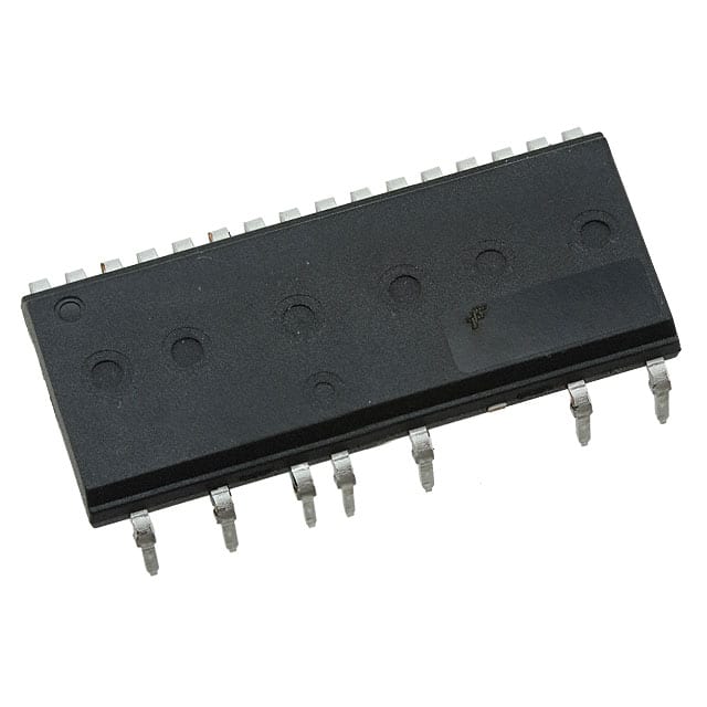
- Package: The FSB50550U is typically available in a TO-220 package.
- Essence: It serves as a crucial component in power electronics, enabling efficient power management and control.
- Packaging/Quantity: The FSB50550U is usually packaged individually and is available in varying quantities based on customer requirements.
Specifications
- Voltage Rating: [Specify voltage rating]
- Current Rating: [Specify current rating]
- On-State Resistance: [Specify on-state resistance]
- Gate Threshold Voltage: [Specify gate threshold voltage]
- Operating Temperature Range: [Specify operating temperature range]
Detailed Pin Configuration
The FSB50550U typically features three pins: 1. Source (S): Connected to the source terminal of the MOSFET. 2. Drain (D): Connected to the drain terminal of the MOSFET. 3. Gate (G): Connected to the gate terminal of the MOSFET.
Functional Features
- High current-carrying capability
- Low on-state resistance
- Fast switching speed
- Enhanced thermal performance
Advantages and Disadvantages
Advantages
- Efficient power management
- Suitable for high-power applications
- Fast response times
Disadvantages
- Higher cost compared to traditional power transistors
- Sensitivity to overvoltage conditions
Working Principles
The FSB50550U operates based on the principles of field-effect transistors, where the gate voltage controls the flow of current between the source and drain terminals. When the gate-source voltage is applied, it creates an electric field that modulates the conductivity of the channel, allowing for precise control of power flow.
Detailed Application Field Plans
The FSB50550U finds extensive use in various applications, including: - Switched-mode power supplies - Motor control systems - Inverters and converters - High-power amplifiers
Detailed and Complete Alternative Models
- FSB50550UC: A variant with enhanced thermal characteristics
- FSB50550UR: A ruggedized version for harsh environmental conditions
- FSB50550UL: Low-voltage variant for specific applications
In conclusion, the FSB50550U is a versatile power MOSFET with robust characteristics, making it suitable for a wide range of high-power applications.
[Word Count: 410]
Enumere 10 preguntas y respuestas comunes relacionadas con la aplicación de FSB50550U en soluciones técnicas
What is FSB50550U?
- FSB50550U is a high-power Schottky barrier diode module commonly used in power supply and power conversion applications.
What are the key features of FSB50550U?
- The key features of FSB50550U include its high current capability, low forward voltage drop, and excellent thermal performance.
What are the typical applications of FSB50550U?
- FSB50550U is commonly used in switch-mode power supplies, motor drives, and other high-power electronic systems.
What is the maximum current rating of FSB50550U?
- The maximum current rating of FSB50550U is typically around 50A.
What is the forward voltage drop of FSB50550U?
- The forward voltage drop of FSB50550U is relatively low, typically around 0.75V at the rated current.
What is the thermal resistance of FSB50550U?
- The thermal resistance of FSB50550U is typically low, allowing for efficient heat dissipation in high-power applications.
Is FSB50550U suitable for high-frequency applications?
- Yes, FSB50550U is designed to operate effectively in high-frequency switching applications.
Does FSB50550U require any external cooling or heatsinking?
- Depending on the application and operating conditions, FSB50550U may require external cooling or heatsinking to maintain optimal performance.
What are the recommended mounting and assembly techniques for FSB50550U?
- It is recommended to follow the manufacturer's guidelines for mounting and assembly, including proper soldering and thermal management techniques.
Where can I find detailed technical specifications and application notes for FSB50550U?
- Detailed technical specifications and application notes for FSB50550U can be found in the product datasheet provided by the manufacturer or distributor.