

Consulte las especificaciones para obtener detalles del producto.
J310ZL1G Product Overview
Introduction
The J310ZL1G is a specialized electronic component belonging to the category of field-effect transistors (FETs). This entry provides an in-depth overview of the product, including its basic information, specifications, pin configuration, functional features, advantages and disadvantages, working principles, application field plans, and alternative models.
Basic Information Overview
- Category: Field-Effect Transistor (FET)
- Use: Amplification and switching of electronic signals
- Characteristics: High input impedance, low noise, and high gain
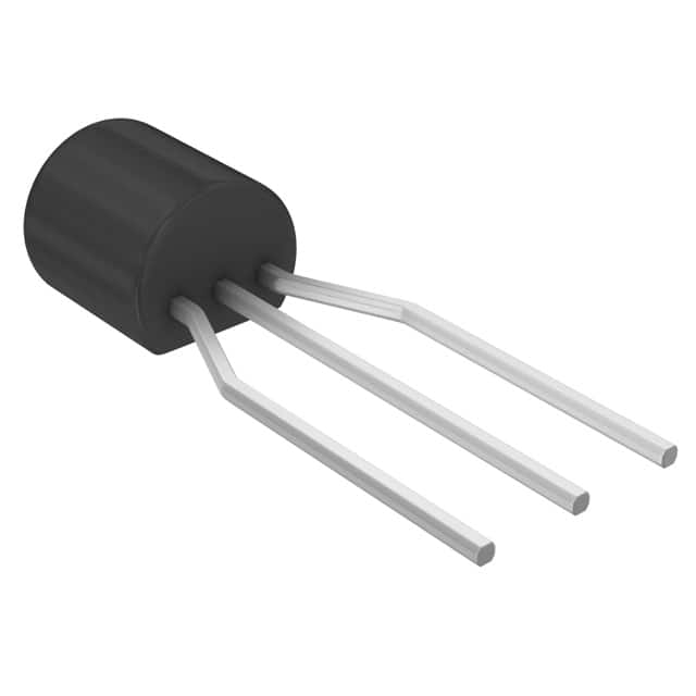
- Package: SOT-23
- Essence: Small-signal amplifier
- Packaging/Quantity: Available in reels with varying quantities
Specifications
- Type: N-Channel
- Maximum Drain-Source Voltage: 25V
- Maximum Gate-Source Voltage: 25V
- Maximum Continuous Drain Current: 10mA
- Power Dissipation: 350mW
- Operating Temperature Range: -55°C to 150°C
Detailed Pin Configuration
The J310ZL1G features three pins: 1. Gate (G): Input terminal for controlling the flow of current 2. Drain (D): Output terminal where the current exits 3. Source (S): Terminal connected to the ground reference or source of input signal
Functional Features
- High input impedance: Allows for minimal loading of preceding stages
- Low noise: Suitable for low-noise amplification applications
- High gain: Enables efficient signal amplification
Advantages and Disadvantages
Advantages
- Low noise figure
- High gain
- Small package size
Disadvantages
- Limited maximum drain-source voltage
- Low continuous drain current rating
Working Principles
The J310ZL1G operates based on the principles of field-effect transistors, utilizing the control of electric fields to modulate the conductivity of a channel.
Detailed Application Field Plans
The J310ZL1G finds extensive use in various applications, including: - Radio frequency (RF) amplifiers - Low-noise preamplifiers - Oscillators - Signal processing circuits
Detailed and Complete Alternative Models
Some alternative models to the J310ZL1G include: - BF862 - J309 - J312
In conclusion, the J310ZL1G serves as a crucial component in electronic circuits, particularly in applications requiring low-noise, high-gain amplification. Its unique characteristics make it suitable for diverse electronic designs, despite its limitations in voltage and current ratings.
Word Count: 320
Enumere 10 preguntas y respuestas comunes relacionadas con la aplicación de J310ZL1G en soluciones técnicas
What is the J310ZL1G?
- The J310ZL1G is a high-frequency, N-channel JFET (junction field-effect transistor) designed for use in RF amplifiers and mixers.
What are the key features of the J310ZL1G?
- The J310ZL1G features low noise, high gain, and excellent linearity, making it suitable for applications in radio frequency circuits.
What are the typical applications of the J310ZL1G?
- The J310ZL1G is commonly used in RF amplifiers, oscillators, mixers, and other high-frequency applications.
What is the maximum power dissipation of the J310ZL1G?
- The maximum power dissipation of the J310ZL1G is typically around 350mW.
What is the operating frequency range of the J310ZL1G?
- The J310ZL1G is designed for operation in the RF frequency range, typically from a few megahertz to several gigahertz.
What are the recommended biasing conditions for the J310ZL1G?
- The J310ZL1G is typically biased in the common-source configuration with appropriate DC biasing to achieve the desired performance.
Does the J310ZL1G require any special handling or precautions during assembly?
- It is important to handle the J310ZL1G with ESD (electrostatic discharge) precautions to prevent damage to the sensitive semiconductor components.
Can the J310ZL1G be used in low-power applications?
- While the J310ZL1G is optimized for high-frequency and high-gain applications, it can also be used in lower power applications with appropriate circuit design.
Are there any known limitations or trade-offs when using the J310ZL1G?
- Like all electronic components, the J310ZL1G has specific trade-offs such as noise figure, gain, and linearity that should be considered in the design process.
Where can I find detailed technical specifications and application notes for the J310ZL1G?
- Detailed technical specifications, application notes, and circuit examples for the J310ZL1G can be found in the manufacturer's datasheet and application guides.