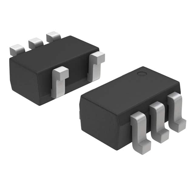
Consulte las especificaciones para obtener detalles del producto.

MC74VHC1G08DFT1G
Product Overview
- Category: Integrated Circuit (IC)
- Use: Logic Gate
- Characteristics: High-speed, low-power consumption
- Package: SOT-353
- Essence: AND Gate
- Packaging/Quantity: Tape and Reel, 3000 pieces per reel
Specifications
- Supply Voltage Range: 2.0V to 5.5V
- Input Voltage Range: 0V to VCC
- Output Voltage Range: 0V to VCC
- Maximum Operating Frequency: 8 MHz
- Propagation Delay: 4.3 ns (typical)
Detailed Pin Configuration
The MC74VHC1G08DFT1G has a total of 5 pins:
- A - Input A
- B - Input B
- GND - Ground
- Y - Output
- VCC - Power Supply
Functional Features
The MC74VHC1G08DFT1G is an AND gate that performs logical multiplication on two input signals. It operates at high speed while consuming low power, making it suitable for various applications.
Advantages and Disadvantages
Advantages: - High-speed operation - Low power consumption - Wide supply voltage range - Small package size
Disadvantages: - Limited number of inputs (only two) - Not suitable for complex logic operations
Working Principles
The MC74VHC1G08DFT1G works based on the principles of digital logic. When both input signals (A and B) are high (logic level 1), the output signal (Y) becomes high as well. In all other cases, the output remains low (logic level 0).
Detailed Application Field Plans
The MC74VHC1G08DFT1G can be used in various applications, including but not limited to: - Digital systems - Microcontrollers - Communication devices - Consumer electronics - Automotive electronics
Detailed and Complete Alternative Models
Some alternative models that can be considered as alternatives to MC74VHC1G08DFT1G are:
- SN74LVC1G08DBVR - AND Gate, SOT-23 package
- CD4081BE - Quad 2-Input AND Gate, DIP-14 package
- 74HC08N - Quad 2-Input AND Gate, DIP-14 package
- HCF4081BE - Quad 2-Input AND Gate, DIP-14 package
These alternative models offer similar functionality and can be used as replacements depending on specific requirements.
In conclusion, the MC74VHC1G08DFT1G is a high-speed, low-power AND gate IC. It is widely used in digital systems, microcontrollers, communication devices, consumer electronics, and automotive electronics. Its small package size and wide supply voltage range make it suitable for various applications. However, it has a limited number of inputs and may not be suitable for complex logic operations.
Enumere 10 preguntas y respuestas comunes relacionadas con la aplicación de MC74VHC1G08DFT1G en soluciones técnicas
Sure! Here are 10 common questions and answers related to the application of MC74VHC1G08DFT1G in technical solutions:
Q1: What is MC74VHC1G08DFT1G? A1: MC74VHC1G08DFT1G is a single 2-input AND gate IC (integrated circuit) that belongs to the VHC (Very High-Speed CMOS) logic family.
Q2: What is the operating voltage range for MC74VHC1G08DFT1G? A2: The operating voltage range for MC74VHC1G08DFT1G is typically between 2.0V and 5.5V.
Q3: What is the maximum output current of MC74VHC1G08DFT1G? A3: The maximum output current of MC74VHC1G08DFT1G is around 8mA.
Q4: Can MC74VHC1G08DFT1G be used in high-speed applications? A4: Yes, MC74VHC1G08DFT1G is designed for high-speed operation and can be used in various high-speed applications.
Q5: What is the package type for MC74VHC1G08DFT1G? A5: MC74VHC1G08DFT1G comes in a small SOT-353 package.
Q6: Is MC74VHC1G08DFT1G compatible with other logic families? A6: Yes, MC74VHC1G08DFT1G is compatible with other CMOS logic families and can be easily integrated into existing designs.
Q7: Can MC74VHC1G08DFT1G handle multiple inputs? A7: No, MC74VHC1G08DFT1G is a 2-input AND gate and can only handle two input signals.
Q8: What is the propagation delay of MC74VHC1G08DFT1G? A8: The propagation delay of MC74VHC1G08DFT1G is typically around 4.5ns.
Q9: Can MC74VHC1G08DFT1G be used in battery-powered applications? A9: Yes, MC74VHC1G08DFT1G has a low power consumption and can be used in battery-powered applications.
Q10: Are there any recommended applications for MC74VHC1G08DFT1G? A10: MC74VHC1G08DFT1G is commonly used in various digital logic circuits, such as signal conditioning, level shifting, and interfacing between different voltage domains.
Please note that these answers are general and may vary depending on specific application requirements and datasheet specifications.

