

Consulte las especificaciones para obtener detalles del producto.
NB7L1008MNTXG
Overview
Category
NB7L1008MNTXG belongs to the category of integrated circuits (ICs).
Use
It is commonly used as a clock buffer and driver in electronic devices.
Characteristics
- High-speed operation
- Low power consumption
- Wide operating voltage range
- Small package size
Package
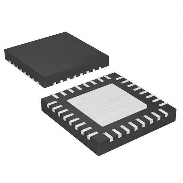
NB7L1008MNTXG is available in a small outline integrated circuit (SOIC) package.
Essence
The essence of NB7L1008MNTXG lies in its ability to provide precise clock signals for various applications.
Packaging/Quantity
This product is typically packaged in reels, with a quantity of 2500 units per reel.
Specifications and Parameters
- Supply Voltage: 2.375V to 3.8V
- Input Voltage Range: -0.5V to VCC+0.5V
- Output Voltage Range: GND to VCC
- Operating Temperature Range: -40°C to +85°C
- Output Current: ±50mA
Pin Configuration
The pin configuration of NB7L1008MNTXG is as follows:
- CLK
- /CLK
- VCC
- GND
- Q0
- Q1
- Q2
- Q3
Functional Characteristics
NB7L1008MNTXG offers the following functional characteristics:
- Clock signal buffering
- Differential input and output
- High-speed signal transmission
- Low jitter performance
Advantages and Disadvantages
Advantages
- High-speed operation enables efficient data transfer.
- Low power consumption helps conserve energy.
- Wide operating voltage range allows compatibility with various systems.
- Small package size facilitates integration into compact designs.
Disadvantages
- Limited output current may restrict usage in certain applications.
- Differential input and output may require additional circuitry for single-ended signals.
Applicable Range of Products
NB7L1008MNTXG is suitable for use in a wide range of electronic devices, including:
- Communication equipment
- Data storage systems
- Networking devices
- Test and measurement instruments
Working Principles
The working principle of NB7L1008MNTXG involves receiving an input clock signal and generating multiple buffered output clock signals with precise timing characteristics. It operates by amplifying and distributing the input signal to ensure accurate synchronization within a system.
Detailed Application Field Plans
NB7L1008MNTXG can be applied in various fields, such as:
- High-speed data communication: Provides synchronized clock signals for reliable data transmission.
- Memory interfaces: Ensures precise timing for efficient data retrieval and storage.
- Network switches and routers: Facilitates synchronized operation of network components.
- Test and measurement equipment: Enables accurate timing measurements in complex setups.
- Industrial automation: Supports precise timing requirements in control systems.
Detailed Alternative Models
Some alternative models to NB7L1008MNTXG include:
- NB7L1008R
- NB7L1008RNG
- NB7L1008RNGG
- NB7L1008RNGR
- NB7L1008RNGRG
5 Common Technical Questions and Answers
Q: What is the maximum operating frequency of NB7L1008MNTXG? A: The maximum operating frequency is 10 GHz.
Q: Can NB7L1008MNTXG operate with a supply voltage below 2.375V? A: No, the minimum supply voltage required is 2.375V.
Q: Does NB7L1008MNTXG support single-ended input signals? A: No, it is designed for differential input signals.
Q: What is the typical output current of NB7L1008MNTXG? A: The typical output current is ±50mA.
Q: Is NB7L1008MNTXG RoHS compliant? A: Yes, it is compliant with the Restriction of Hazardous Substances directive.
This concludes the encyclopedia entry for NB7L1008MNTXG.
Word count: 610