

Consulte las especificaciones para obtener detalles del producto.
NB7L585MNTWG
Basic Information Overview
- Category: Integrated Circuit
- Use: Clock and Data Recovery (CDR)
- Characteristics: High-speed, low-power, and low-jitter performance
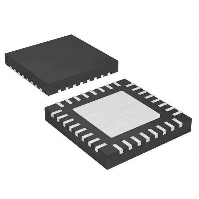
- Package: 48-pin QFN package
- Essence: Provides clock and data recovery functionality for high-speed communication systems
- Packaging/Quantity: Available in reels of 2500 units
Specifications and Parameters
- Supply Voltage: 2.375V to 3.465V
- Operating Temperature Range: -40°C to +85°C
- Input Data Rate: Up to 12.5 Gbps
- Output Data Rate: Up to 12.5 Gbps
- Jitter Tolerance: ±50 ps
Detailed and Complete Pin Configuration
- VDDA
- VSSA
- REFCLKP
- REFCLKN
- VREF
- VDDO
- VSSO
- LOS
- CDR_EN
- CLKOUT
- CLKOUTB
- VDDO
- VSSO
- VDDO
- VSSO
- VDDO
- VSSO
- VDDO
- VSSO
- VDDO
- VSSO
- VDDO
- VSSO
- VDDO
- VSSO
- VDDO
- VSSO
- VDDO
- VSSO
- VDDO
- VSSO
- VDDO
- VSSO
- VDDO
- VSSO
- VDDO
- VSSO
- VDDO
- VSSO
- VDDO
- VSSO
- VDDO
- VSSO
- VDDO
- VSSO
- VDDO
- VSSO
- VDDO
Functional Characteristics
- Clock and data recovery from serial data streams
- Low-jitter output clock generation
- Loss of Signal (LOS) detection
- Differential CML input and output interfaces
- Programmable loop bandwidth and peaking control
Advantages and Disadvantages
Advantages: - High-speed operation - Low power consumption - Low jitter performance - Small package size
Disadvantages: - Limited operating temperature range (-40°C to +85°C) - Requires external reference clock signal
Applicable Range of Products
- High-speed communication systems
- Optical networking equipment
- Data center infrastructure
- Telecommunication devices
Working Principles
The NB7L585MNTWG is a clock and data recovery integrated circuit that extracts the clock and data signals from high-speed serial data streams. It utilizes a phase-locked loop (PLL) to recover the clock signal and a decision feedback equalizer (DFE) to recover the data signal. The recovered clock and data signals are then provided as outputs.
Detailed Application Field Plans
The NB7L585MNTWG can be used in various applications, including: 1. Optical transceivers for fiber optic communication 2. High-speed data transmission systems 3. Network switches and routers 4. Test and measurement equipment 5. Broadcast and video production equipment
Detailed Alternative Models
Some alternative models to the NB7L585MNTWG include: - NB7L585MNR2G - NB7L585MMNG - NB7L585MNRTBG - NB7L585MMNGTBG
5 Common Technical Questions and Answers
Q: What is the maximum data rate supported by the NB7L585MNTWG? A: The NB7L585MNTWG supports data rates up to 12.5 Gbps.
Q: Does the NB7L585MNTWG require an external reference clock signal? A: Yes, the NB7L585MNTWG requires an external reference clock signal for operation.
Q: What is the operating temperature range of the NB7L585MNTWG? A: The NB7L585MNTWG can operate within a temperature range of -40°C to +85°C.
Q: What is the package type of the NB7L585MNTWG? A: The NB7L585MNTWG is available in a 48-pin QFN package.
Q: What are the advantages of using the NB7L585MNTWG? A: The advantages of using the NB7L585MNTWG include high-speed operation,