

Consulte las especificaciones para obtener detalles del producto.
NC7SV126L6X
Product Overview
- Category: Integrated Circuit (IC)
- Use: Logic Gate
- Characteristics: Low Voltage, Single Supply, Non-Inverting Buffer
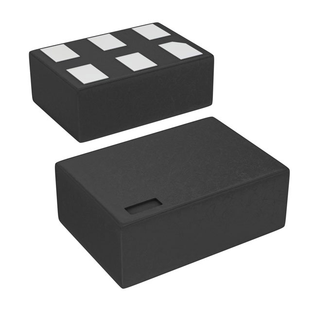
- Package: SOT-23-6
- Essence: High-speed CMOS technology
- Packaging/Quantity: Tape and Reel, 3000 pieces per reel
Specifications
- Supply Voltage Range: 1.65V to 5.5V
- Input Voltage Range: GND to VCC
- Output Voltage Range: GND to VCC
- Maximum Quiescent Current: 1μA
- Maximum Propagation Delay: 2.5ns
- Maximum Operating Frequency: 200MHz
Detailed Pin Configuration
The NC7SV126L6X has a total of 6 pins arranged as follows:
____
   1 -|    |- 6
   2 -|    |- 5
   3 -|    |- 4
      ------
Pin Description: 1. A: Input A 2. Y: Output Y 3. GND: Ground 4. B: Input B 5. Y: Output Y 6. VCC: Power Supply
Functional Features
- Non-inverting buffer with high-speed performance
- Supports wide supply voltage range for versatile applications
- Low quiescent current makes it suitable for battery-powered devices
- Provides reliable logic level translation between different voltage domains
Advantages
- Small form factor package allows for space-efficient designs
- Wide operating voltage range enables compatibility with various systems
- Low power consumption extends battery life in portable devices
- High-speed operation facilitates rapid data processing
Disadvantages
- Limited number of inputs and outputs restricts complex circuit designs
- Sensitivity to electrostatic discharge (ESD) requires proper handling during assembly and usage
Working Principles
The NC7SV126L6X is a non-inverting buffer that amplifies and reproduces the input signal at its output. It operates using high-speed CMOS technology, which ensures fast switching times and low power consumption. The device can be powered by a single supply voltage ranging from 1.65V to 5.5V, making it compatible with a wide range of applications.
Detailed Application Field Plans
The NC7SV126L6X is commonly used in various digital systems where logic level translation and buffering are required. Some specific application fields include:
- Mobile Devices: Used for level shifting between different voltage domains in smartphones, tablets, and wearable devices.
- Communication Systems: Employed in signal conditioning circuits for reliable data transmission between different components.
- Industrial Automation: Integrated into control systems to interface between different logic families and voltage levels.
- Automotive Electronics: Utilized for voltage level translation in automotive control units and infotainment systems.
- Consumer Electronics: Incorporated in audio/video equipment, gaming consoles, and home automation devices for signal buffering and level conversion.
Detailed and Complete Alternative Models
- SN74LVC1G125DBVR: Single Buffer Gate, Non-Inverting, 1-Channel, SOT-23-5 package.
- MC74VHC1GT125DF1G: Single Buffer Gate, Non-Inverting, 1-Channel, SOT-353 package.
- TC7SZ126AFK(TE85L,F): Single Buffer Gate, Non-Inverting, 1-Channel, SOT-353 package.
These alternative models offer similar functionality and characteristics to the NC7SV126L6X and can be considered as substitutes depending on specific requirements.
Word count: 445 words
Enumere 10 preguntas y respuestas comunes relacionadas con la aplicación de NC7SV126L6X en soluciones técnicas
Sure! Here are 10 common questions and answers related to the application of NC7SV126L6X in technical solutions:
Question: What is the NC7SV126L6X?
Answer: The NC7SV126L6X is a single buffer gate with 3-state output, commonly used in digital logic circuits.Question: What is the voltage range supported by NC7SV126L6X?
Answer: The NC7SV126L6X supports a voltage range from 1.65V to 5.5V.Question: What is the maximum output current of NC7SV126L6X?
Answer: The maximum output current of NC7SV126L6X is typically around 32mA.Question: Can I use NC7SV126L6X for level shifting applications?
Answer: Yes, NC7SV126L6X can be used for level shifting between different voltage domains.Question: Is NC7SV126L6X suitable for bidirectional communication?
Answer: No, NC7SV126L6X is a unidirectional buffer and not suitable for bidirectional communication.Question: What is the propagation delay of NC7SV126L6X?
Answer: The propagation delay of NC7SV126L6X is typically around 2.5ns.Question: Can I connect multiple NC7SV126L6X devices in parallel?
Answer: Yes, you can connect multiple NC7SV126L6X devices in parallel to increase the output drive capability.Question: Does NC7SV126L6X have built-in ESD protection?
Answer: Yes, NC7SV126L6X has built-in ESD protection to safeguard against electrostatic discharge.Question: Can NC7SV126L6X be used in high-speed applications?
Answer: Yes, NC7SV126L6X can be used in high-speed applications due to its low propagation delay.Question: What is the package type of NC7SV126L6X?
Answer: NC7SV126L6X is available in a SOT-23-6 package, which is small and suitable for space-constrained designs.
Please note that the answers provided here are general and may vary depending on specific datasheet specifications and application requirements.