

Consulte las especificaciones para obtener detalles del producto.
NC7WZ07L6X
Product Overview
- Category: Integrated Circuit (IC)
- Use: Logic Gate Buffer/Driver
- Characteristics: Low Voltage, High-Speed, Dual Buffer/Driver
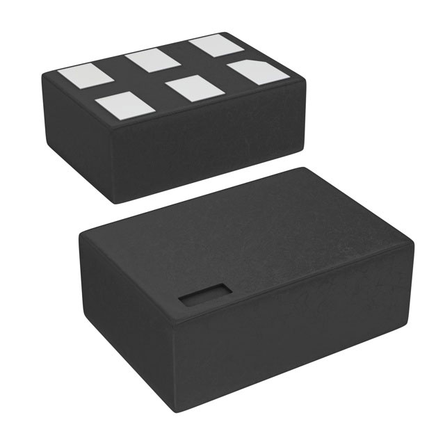
- Package: SOT-23-6
- Essence: The NC7WZ07L6X is a dual buffer/driver IC designed for low voltage applications. It provides high-speed signal buffering and driving capabilities.
- Packaging/Quantity: Available in tape and reel packaging with 3000 units per reel.
Specifications
- Supply Voltage: 1.65V to 5.5V
- Input Voltage: 0V to VCC
- Output Voltage: 0V to VCC
- Operating Temperature Range: -40°C to +85°C
- Propagation Delay: 2.5ns (typical)
- Output Current: ±24mA
Detailed Pin Configuration
The NC7WZ07L6X has a total of six pins arranged as follows:
___________
   VCC | 1     6 | GND
   A1  | 2     5 | Y1
   A2  | 3     4 | Y2
       ‾‾‾‾‾‾‾‾‾‾‾‾
Functional Features
- Dual Buffer/Driver: The NC7WZ07L6X contains two independent buffer/driver circuits in a single package.
- Low Voltage Operation: It operates at a supply voltage as low as 1.65V, making it suitable for low power and portable applications.
- High-Speed Operation: With a propagation delay of only 2.5ns, it ensures fast signal buffering and driving.
- Wide Input and Output Voltage Range: The IC can accept input signals from 0V to VCC and provide output signals within the same voltage range.
- High Output Current: It can source or sink up to ±24mA of current, allowing it to drive capacitive loads efficiently.
Advantages and Disadvantages
Advantages: - Low voltage operation enables energy-efficient designs. - High-speed operation ensures quick signal processing. - Dual buffer/driver configuration provides flexibility in circuit design. - Wide input and output voltage range allows compatibility with various systems. - High output current capability enables driving of capacitive loads.
Disadvantages: - Limited number of buffer/driver circuits in a single package. - Not suitable for high voltage applications.
Working Principles
The NC7WZ07L6X is based on complementary metal-oxide-semiconductor (CMOS) technology. It utilizes a combination of NMOS and PMOS transistors to achieve low voltage operation and high-speed performance. The input signals are buffered and amplified by the internal circuitry, providing clean and reliable output signals.
Detailed Application Field Plans
The NC7WZ07L6X is commonly used in various electronic systems that require signal buffering and driving at low voltages. Some typical application fields include:
- Portable Devices: It can be used in smartphones, tablets, and other battery-powered devices to buffer and drive signals between different components.
- Communication Systems: The IC finds applications in communication systems such as routers, switches, and network equipment to ensure proper signal transmission.
- Industrial Control Systems: It can be employed in industrial control systems to interface between low voltage sensors and actuators.
- Automotive Electronics: The NC7WZ07L6X can be utilized in automotive electronics for signal conditioning and driving purposes.
Detailed and Complete Alternative Models
- SN74LVC07A: This is a similar dual buffer/driver IC from Texas Instruments. It operates at a supply voltage of 1.65V to 5.5V and offers comparable performance to the NC7WZ07L6X.
- MC74LVX07: Another alternative from ON Semiconductor, the MC74LVX07 is a dual buffer/driver IC with a supply voltage range of 2V to 3.6V. It provides similar functionality to the NC7WZ07L6X.
These alternative models can be considered based on specific requirements and availability.
Word count: 457 words
Enumere 10 preguntas y respuestas comunes relacionadas con la aplicación de NC7WZ07L6X en soluciones técnicas
Sure! Here are 10 common questions and answers related to the application of NC7WZ07L6X in technical solutions:
Question: What is NC7WZ07L6X?
Answer: NC7WZ07L6X is a high-performance dual buffer with open-drain outputs, commonly used in digital logic applications.Question: What is the voltage supply range for NC7WZ07L6X?
Answer: The voltage supply range for NC7WZ07L6X is typically between 1.65V and 5.5V.Question: Can NC7WZ07L6X be used as a level shifter?
Answer: Yes, NC7WZ07L6X can be used as a level shifter to convert signals between different voltage levels.Question: What is the maximum data rate supported by NC7WZ07L6X?
Answer: NC7WZ07L6X supports a maximum data rate of up to 100 MHz.Question: Is NC7WZ07L6X suitable for bidirectional communication?
Answer: Yes, NC7WZ07L6X is designed for bidirectional communication and can be used for both input and output signals.Question: Can NC7WZ07L6X be used in battery-powered devices?
Answer: Yes, NC7WZ07L6X has a low power consumption and can be used in battery-powered devices.Question: What is the typical propagation delay of NC7WZ07L6X?
Answer: The typical propagation delay of NC7WZ07L6X is around 4 ns.Question: Does NC7WZ07L6X have built-in ESD protection?
Answer: Yes, NC7WZ07L6X has built-in ESD protection to safeguard against electrostatic discharge.Question: Can NC7WZ07L6X be used in automotive applications?
Answer: Yes, NC7WZ07L6X is suitable for automotive applications and meets the required standards.Question: Are there any recommended application circuits for NC7WZ07L6X?
Answer: Yes, the datasheet of NC7WZ07L6X provides recommended application circuits that can be used as a reference for various technical solutions.
Please note that the answers provided here are general and may vary depending on specific use cases and requirements. It's always recommended to refer to the datasheet and consult with the manufacturer for detailed information.