

Consulte las especificaciones para obtener detalles del producto.
NCP1247AD100R2G
Overview
Product Category: Integrated Circuit (IC)
Use: Power Management IC
Characteristics: - High voltage startup - Current mode control - Frequency jittering for EMI reduction - Built-in protection features - Low standby power consumption
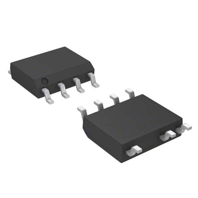
Package: SOIC-8
Essence: The NCP1247AD100R2G is a power management IC designed for offline flyback converters. It integrates various functions required for efficient power conversion and offers reliable performance.
Packaging/Quantity: The NCP1247AD100R2G is available in a standard SOIC-8 package. It is typically sold in reels of 2500 units.
Specifications
- Input Voltage Range: 85V to 265V AC
- Output Power: Up to 10W
- Switching Frequency: 65kHz (typical)
- Startup Current: 25µA (typical)
- Operating Temperature Range: -40°C to +125°C
Pin Configuration
The NCP1247AD100R2G has the following pin configuration:
- VCC: Supply voltage input
- GND: Ground reference
- FB: Feedback pin for output voltage regulation
- COMP: Compensation pin for loop stability
- CS: Current sense input for current mode control
- DRAIN: Drain pin for power MOSFET connection
- VSTR: Voltage startup pin for high voltage startup
- NC: No Connection
Functional Features
- High voltage startup enables operation in wide input voltage range
- Current mode control provides excellent line and load regulation
- Frequency jittering reduces electromagnetic interference (EMI)
- Built-in protection features include overvoltage, overcurrent, and overtemperature protection
- Low standby power consumption enhances energy efficiency
Advantages and Disadvantages
Advantages: - Wide input voltage range allows for universal AC input compatibility - Excellent line and load regulation ensures stable output voltage - Frequency jittering reduces EMI, meeting regulatory standards - Built-in protection features enhance system reliability - Low standby power consumption improves energy efficiency
Disadvantages: - Limited output power of up to 10W may not be suitable for high-power applications - SOIC-8 package may require additional thermal management for higher power dissipation
Working Principles
The NCP1247AD100R2G operates as a flyback converter, which is a type of switched-mode power supply. It uses a power MOSFET to switch the primary side of the transformer, creating an oscillating current. This current is then transferred to the secondary side of the transformer, where it is rectified and filtered to provide the desired output voltage.
The IC utilizes current mode control to regulate the output voltage. By sensing the current flowing through the power MOSFET, it adjusts the duty cycle of the switching waveform to maintain a stable output voltage despite variations in input voltage and load conditions.
Detailed Application Field Plans
The NCP1247AD100R2G is commonly used in various low-power applications, including but not limited to: - Power adapters - Battery chargers - LED lighting - Home appliances - Industrial equipment
Alternative Models
Here are some alternative models that can be considered as replacements for the NCP1247AD100R2G: - NCP1247AD65R2G - NCP1247AD80R2G - NCP1247AD120R2G
These models offer similar functionality and performance characteristics, but with different output power ratings.
In conclusion, the NCP1247AD100R2G is a versatile power management IC suitable for low-power applications. Its integrated features, wide input voltage range, and protection mechanisms make it a reliable choice for various power conversion needs.
Enumere 10 preguntas y respuestas comunes relacionadas con la aplicación de NCP1247AD100R2G en soluciones técnicas
Sure! Here are 10 common questions and answers related to the application of NCP1247AD100R2G in technical solutions:
Q: What is NCP1247AD100R2G? A: NCP1247AD100R2G is a high-performance integrated circuit (IC) designed for offline flyback converters used in power supply applications.
Q: What is the input voltage range of NCP1247AD100R2G? A: The input voltage range of NCP1247AD100R2G is typically between 85V and 265V AC.
Q: What is the maximum output power that NCP1247AD100R2G can handle? A: NCP1247AD100R2G can handle a maximum output power of up to 25W.
Q: Can NCP1247AD100R2G be used in both isolated and non-isolated power supply designs? A: Yes, NCP1247AD100R2G can be used in both isolated and non-isolated power supply designs.
Q: What is the typical switching frequency of NCP1247AD100R2G? A: The typical switching frequency of NCP1247AD100R2G is around 65 kHz.
Q: Does NCP1247AD100R2G have built-in protection features? A: Yes, NCP1247AD100R2G has various built-in protection features such as overvoltage protection, overcurrent protection, and thermal shutdown.
Q: Can NCP1247AD100R2G operate in continuous or discontinuous mode? A: NCP1247AD100R2G can operate in both continuous and discontinuous mode, depending on the load conditions.
Q: What is the maximum duty cycle of NCP1247AD100R2G? A: The maximum duty cycle of NCP1247AD100R2G is typically around 75%.
Q: Is NCP1247AD100R2G suitable for low-power applications? A: Yes, NCP1247AD100R2G is suitable for low-power applications as it can handle output powers as low as a few watts.
Q: Are there any application notes or reference designs available for NCP1247AD100R2G? A: Yes, ON Semiconductor provides application notes and reference designs that can help in implementing NCP1247AD100R2G in various technical solutions.
Please note that the answers provided here are general and may vary based on specific design requirements and application considerations. It is always recommended to refer to the datasheet and relevant documentation for accurate information.