

Consulte las especificaciones para obtener detalles del producto.
NLVAS4599DTT1G
Basic Information Overview
- Category: Integrated Circuit (IC)
- Use: Voltage Level Translator
- Characteristics:
- Bidirectional voltage translation between two different voltage levels
- Low power consumption
- Small form factor
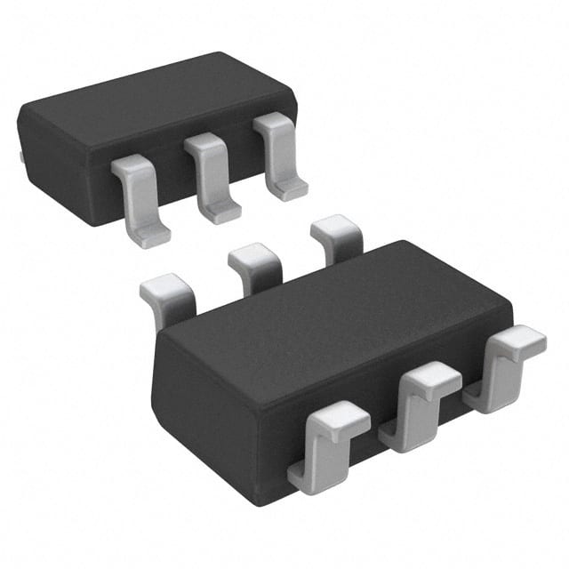
- Package: SOT-23
- Essence: Translates logic level signals between different voltage domains
- Packaging/Quantity: Tape and Reel, 3000 units per reel
Specifications
- Supply Voltage Range: 1.2V to 3.6V
- Logic Voltage Levels: 1.8V to 5.5V
- Maximum Data Rate: 100 Mbps
- Operating Temperature Range: -40°C to +85°C
Detailed Pin Configuration
The NLVAS4599DTT1G has a total of 6 pins: 1. VCCA: Power supply for the A-side logic level (1.2V to 3.6V) 2. VCCB: Power supply for the B-side logic level (1.2V to 3.6V) 3. A1: Input/output pin for the A-side logic level 4. A2: Input/output pin for the A-side logic level 5. B1: Input/output pin for the B-side logic level 6. B2: Input/output pin for the B-side logic level
Functional Features
- Bidirectional voltage translation: Allows seamless communication between devices operating at different voltage levels.
- Automatic direction sensing: Determines the direction of data flow and adjusts the voltage translation accordingly.
- Fast data rate: Supports high-speed data transmission up to 100 Mbps.
- Low power consumption: Designed to minimize power consumption, making it suitable for battery-powered applications.
- ESD protection: Provides Electrostatic Discharge (ESD) protection to safeguard against damage from static electricity.
Advantages
- Compact size: The SOT-23 package offers a small form factor, making it suitable for space-constrained applications.
- Wide voltage range: Supports a wide range of supply and logic voltage levels, providing flexibility in various system designs.
- High-speed data transmission: Capable of handling high data rates, enabling efficient communication between different voltage domains.
- ESD protection: Offers built-in protection against electrostatic discharge, enhancing the reliability of the circuit.
Disadvantages
- Limited current drive capability: The NLVAS4599DTT1G has a limited current drive capability, which may restrict its use in certain applications requiring higher current levels.
- Temperature limitations: The operating temperature range is limited to -40°C to +85°C, which may not be suitable for extreme temperature environments.
Working Principles
The NLVAS4599DTT1G utilizes a combination of MOSFETs and level-shifting circuitry to achieve bidirectional voltage translation. It automatically detects the direction of data flow and adjusts the voltage levels accordingly, ensuring seamless communication between devices operating at different voltage domains.
Detailed Application Field Plans
The NLVAS4599DTT1G finds applications in various fields, including: - Mobile devices: Enables communication between different voltage domains within smartphones, tablets, and wearables. - IoT devices: Facilitates voltage translation between sensors, microcontrollers, and communication modules in IoT applications. - Industrial automation: Allows interfacing between different voltage levels in control systems, PLCs, and motor drives. - Consumer electronics: Used in audio/video equipment, gaming consoles, and home automation systems for voltage level translation.
Detailed and Complete Alternative Models
- TXS0102: Bidirectional voltage-level translator with automatic direction sensing and multiple package options.
- SN74LVC1T45: Single-bit dual-supply bus transceiver with configurable voltage translation and small form factor.
- PCA9306: Dual bidirectional I2C-bus and SMBus voltage-level translator with adjustable voltage levels.
Note: The above alternative models are provided for reference and may have different specifications and features. It is recommended to review the datasheets for detailed information.
Word count: 489 words
Enumere 10 preguntas y respuestas comunes relacionadas con la aplicación de NLVAS4599DTT1G en soluciones técnicas
Sure! Here are 10 common questions and answers related to the application of NLVAS4599DTT1G in technical solutions:
Q1: What is NLVAS4599DTT1G? A1: NLVAS4599DTT1G is a specific model number for a voltage level translator IC (integrated circuit) manufactured by a particular company.
Q2: What is the purpose of NLVAS4599DTT1G? A2: The purpose of NLVAS4599DTT1G is to translate voltage levels between different logic families or voltage domains in electronic circuits.
Q3: What voltage levels can NLVAS4599DTT1G translate? A3: NLVAS4599DTT1G can translate voltage levels between, for example, 3.3V and 5V logic levels.
Q4: How does NLVAS4599DTT1G achieve voltage level translation? A4: NLVAS4599DTT1G uses built-in circuitry to convert input signals from one voltage level to another, ensuring compatibility between different parts of a circuit.
Q5: Can NLVAS4599DTT1G be used bidirectionally? A5: Yes, NLVAS4599DTT1G can be used bidirectionally, meaning it can translate voltage levels in both directions.
Q6: What are some typical applications of NLVAS4599DTT1G? A6: NLVAS4599DTT1G is commonly used in various technical solutions, such as interfacing microcontrollers with different voltage requirements, level shifting in communication interfaces, and mixed-voltage system designs.
Q7: What is the maximum data rate supported by NLVAS4599DTT1G? A7: The maximum data rate supported by NLVAS4599DTT1G depends on various factors, but it can typically handle data rates up to several megabits per second.
Q8: What is the power supply voltage range for NLVAS4599DTT1G? A8: The power supply voltage range for NLVAS4599DTT1G is usually specified in the datasheet provided by the manufacturer. It typically supports a wide range of voltages, such as 1.2V to 5.5V.
Q9: Are there any limitations or considerations when using NLVAS4599DTT1G? A9: Yes, some considerations include ensuring proper signal integrity, understanding the voltage level requirements of the devices being connected, and taking into account the maximum data rate supported by NLVAS4599DTT1G.
Q10: Where can I find more information about NLVAS4599DTT1G? A10: You can find more detailed information about NLVAS4599DTT1G in the datasheet provided by the manufacturer or by visiting their official website.