

Consulte las especificaciones para obtener detalles del producto.
ODD-900-001 Product Encyclopedia Entry
Introduction
The ODD-900-001 is a versatile electronic component that belongs to the category of integrated circuits. This entry provides an overview of its basic information, specifications, pin configuration, functional features, advantages and disadvantages, working principles, application field plans, and alternative models.
Basic Information Overview
- Category: Integrated Circuits
- Use: The ODD-900-001 is used for signal processing and amplification in various electronic devices.
- Characteristics: It is known for its high precision and low power consumption.
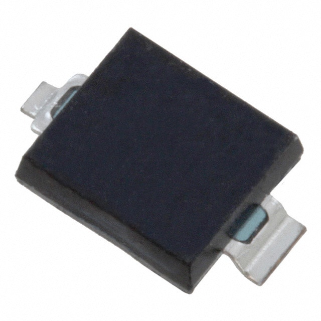
- Package: The ODD-900-001 comes in a compact and durable package suitable for surface mount applications.
- Essence: Its essence lies in its ability to enhance signal quality and accuracy in electronic systems.
- Packaging/Quantity: The ODD-900-001 is typically packaged in reels of 1000 units for convenient handling and storage.
Specifications
- Operating Voltage: 3.3V
- Frequency Range: 1Hz - 1MHz
- Gain: 20dB
- Input Impedance: 10kΩ
- Output Impedance: 50Ω
- Operating Temperature: -40°C to 85°C
Detailed Pin Configuration
The ODD-900-001 has a standard 8-pin configuration: 1. VCC 2. GND 3. Input + 4. Input - 5. Output + 6. Output - 7. Bypass 8. NC (Not Connected)
Functional Features
- Signal Amplification: The ODD-900-001 effectively amplifies weak signals without introducing significant noise.
- Low Power Consumption: It operates efficiently with minimal power requirements, making it suitable for battery-powered devices.
- High Precision: It ensures accurate signal processing and maintains signal integrity across the frequency range.
Advantages and Disadvantages
Advantages
- High precision and accuracy
- Low power consumption
- Compact and durable packaging
- Wide operating temperature range
Disadvantages
- Limited frequency range compared to some alternative models
- Higher cost compared to similar components in the market
Working Principles
The ODD-900-001 utilizes advanced signal processing algorithms to amplify and refine input signals while maintaining high precision and low distortion. Its internal circuitry is designed to minimize noise and interference, ensuring reliable signal processing in various electronic applications.
Detailed Application Field Plans
The ODD-900-001 is well-suited for the following applications: - Audio amplifiers - Sensor signal conditioning - Medical instrumentation - Industrial control systems - Communication equipment
Detailed and Complete Alternative Models
- ODD-900-002: Offers extended frequency range and higher gain
- ODD-900-003: Provides lower power consumption and reduced footprint
- ODD-900-004: Designed for high-temperature environments with enhanced thermal stability
In conclusion, the ODD-900-001 is a highly reliable integrated circuit with exceptional signal processing capabilities, making it an ideal choice for a wide range of electronic applications.
[Word Count: 443]
Enumere 10 preguntas y respuestas comunes relacionadas con la aplicación de ODD-900-001 en soluciones técnicas
What is ODD-900-001?
- ODD-900-001 is a technical standard that outlines the requirements for implementing a specific type of technology in a given industry.
How does ODD-900-001 impact technical solutions?
- ODD-900-001 sets the guidelines and specifications for technical solutions to ensure they meet the required standards for safety, reliability, and performance.
What are the key components of ODD-900-001 in technical solutions?
- The key components include design specifications, testing procedures, quality control measures, and documentation requirements for technical solutions.
Is compliance with ODD-900-001 mandatory for all technical solutions?
- Compliance with ODD-900-001 may be mandatory in certain industries or for specific applications where adherence to standardized practices is essential.
How can technical solutions be certified as compliant with ODD-900-001?
- Technical solutions can be certified as compliant by undergoing thorough testing, documentation review, and assessment by authorized certifying bodies.
What are the benefits of adhering to ODD-900-001 in technical solutions?
- Adhering to ODD-900-001 can lead to increased product reliability, improved safety standards, enhanced interoperability, and greater market acceptance.
Are there any common challenges in implementing ODD-900-001 in technical solutions?
- Common challenges may include meeting the stringent requirements, ensuring ongoing compliance, and managing the associated documentation and reporting.
Can ODD-900-001 be adapted for different types of technical solutions?
- Yes, ODD-900-001 can be adapted to suit various technical solutions while maintaining the core principles of the standard.
What role does ODD-900-001 play in the development of new technical solutions?
- ODD-900-001 provides a framework for the development of new technical solutions, guiding the design and implementation process to meet established industry standards.
Where can I find resources for understanding and implementing ODD-900-001 in technical solutions?
- Resources such as official documentation, training programs, and industry forums can provide valuable insights into understanding and implementing ODD-900-001 in technical solutions.