

Consulte las especificaciones para obtener detalles del producto.
BD3433K-E2
Overview
- Category: Electronic Component
- Use: Power Management
- Characteristics: High Efficiency, Compact Size
- Package: SMD (Surface Mount Device)
- Essence: Voltage Regulator
- Packaging/Quantity: Tape and Reel, 1000 pieces per reel
Specifications and Parameters
- Input Voltage Range: 4.5V to 24V
- Output Voltage Range: 1.2V to 5.5V
- Maximum Output Current: 3A
- Operating Temperature Range: -40°C to +85°C
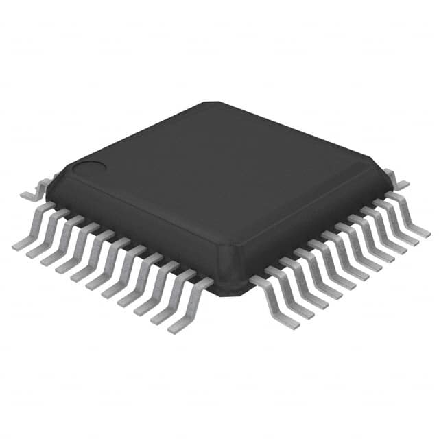
- Package Type: SOP-8
Pin Configuration
The BD3433K-E2 has a total of 8 pins arranged as follows:
```
| 1 2 3 4 | | 5 6 7 8 |
```
Pin Description: 1. VIN: Input Voltage 2. GND: Ground 3. EN: Enable Pin 4. FB: Feedback Pin 5. SW: Switching Node 6. PGND: Power Ground 7. VOUT: Output Voltage 8. COMP: Compensation Pin
Functional Characteristics
- Efficient voltage regulation for various applications
- Overcurrent protection
- Thermal shutdown protection
- Soft start function
- Adjustable output voltage
Advantages
- High efficiency resulting in reduced power consumption
- Compact size suitable for space-constrained designs
- Wide input voltage range for versatile applications
- Robust overcurrent and thermal protection features
- Easy to integrate into existing circuits
Disadvantages
- Limited maximum output current of 3A
- Operating temperature range may not be suitable for extreme environments
Applicable Range of Products
The BD3433K-E2 is commonly used in electronic devices that require efficient voltage regulation, such as: - Mobile phones - Tablets - Portable gaming consoles - IoT devices
Working Principles
The BD3433K-E2 is a voltage regulator that takes an input voltage and provides a stable output voltage. It achieves this by using internal circuitry to monitor the input and output voltages, adjusting the switching frequency of the internal power MOSFET accordingly.
Detailed Application Field Plans
The BD3433K-E2 can be used in various applications, including: 1. Mobile phone power management 2. Battery-powered devices 3. Industrial automation systems 4. Automotive electronics 5. LED lighting systems
Detailed Alternative Models
Some alternative models to the BD3433K-E2 include: - BD3433K-F2 - BD3433K-G2 - BD3433K-H2
5 Common Technical Questions and Answers
Q: What is the maximum output current of the BD3433K-E2? A: The maximum output current is 3A.
Q: Can the BD3433K-E2 operate in extreme temperatures? A: The operating temperature range is -40°C to +85°C, which covers most common operating conditions.
Q: Is the output voltage adjustable? A: Yes, the output voltage can be adjusted within the range of 1.2V to 5.5V.
Q: Does the BD3433K-E2 have overcurrent protection? A: Yes, it has built-in overcurrent protection to safeguard against excessive current draw.
Q: What package type does the BD3433K-E2 come in? A: It comes in a SOP-8 package, which is a surface mount device package.
This encyclopedia entry provides an overview of the BD3433K-E2, including its basic information, specifications, pin configuration, functional characteristics, advantages and disadvantages, applicable range of products, working principles, detailed application field plans, alternative models, and common technical questions and answers.