

Consulte las especificaciones para obtener detalles del producto.
L612F Product Overview
Introduction
The L612F is a versatile electronic component that belongs to the category of integrated circuits. This semiconductor device is widely used in various electronic applications due to its unique characteristics and functional features.
Basic Information Overview
- Category: Integrated Circuit
- Use: Signal Processing, Amplification
- Characteristics: High Gain, Low Noise, Wide Frequency Range
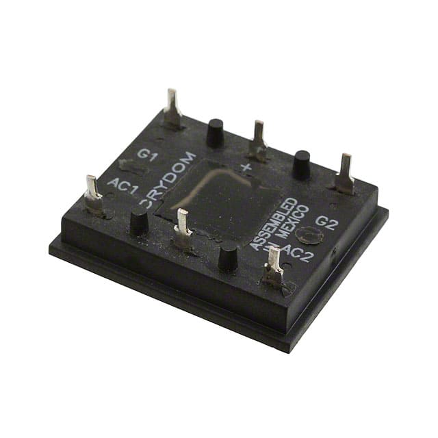
- Package: DIP (Dual Inline Package)
- Essence: Amplification and Signal Conditioning
- Packaging/Quantity: Typically available in reels of 1000 units
Specifications
The L612F integrated circuit has the following specifications: - Input Voltage Range: 3V to 15V - Operating Temperature: -40°C to 85°C - Gain Bandwidth Product: 10MHz - Input Bias Current: 10nA - Output Voltage Swing: ±12V
Detailed Pin Configuration
The L612F integrated circuit has a standard pin configuration with the following key pins: 1. Pin 1: Input 2. Pin 2: Ground 3. Pin 3: Output 4. Pin 4: Vcc
Functional Features
The L612F offers the following functional features: - High voltage gain - Low input bias current - Wide bandwidth - Low output impedance - Stable performance over temperature variations
Advantages and Disadvantages
Advantages
- Versatile application in signal processing
- Low noise amplification
- Wide operating voltage range
Disadvantages
- Limited output current capability
- Sensitivity to electromagnetic interference
Working Principles
The L612F operates based on the principles of amplification and signal conditioning. It utilizes internal circuitry to amplify and process input signals with high fidelity and minimal distortion.
Detailed Application Field Plans
The L612F finds extensive use in the following application fields: - Audio Amplification - Sensor Signal Conditioning - Communication Systems - Instrumentation
Detailed and Complete Alternative Models
Some alternative models to the L612F include: - LM358 - TL081 - OP07 - AD822
In conclusion, the L612F integrated circuit offers a reliable solution for signal processing and amplification applications, with its unique characteristics and functional features making it a preferred choice in various electronic systems.
Word Count: 298
Enumere 10 preguntas y respuestas comunes relacionadas con la aplicación de L612F en soluciones técnicas
What is L612F?
- L612F is a specific type of component or material used in technical solutions, often in electronic or mechanical systems.
What are the key features of L612F?
- L612F is known for its high durability, resistance to temperature fluctuations, and excellent electrical conductivity.
How is L612F typically used in technical solutions?
- L612F is commonly used as a critical part of circuit boards, connectors, or as a coating for components to enhance their performance and longevity.
What are the advantages of using L612F in technical solutions?
- The use of L612F can lead to improved reliability, reduced maintenance needs, and enhanced overall performance of the technical system.
Are there any limitations or considerations when using L612F?
- It's important to consider the compatibility of L612F with other materials and the specific environmental conditions in which it will be used.
Where can L612F be sourced from?
- L612F may be available through specialized suppliers or manufacturers that cater to the technical and engineering industries.
What are some common alternatives to L612F?
- Depending on the specific requirements, alternatives to L612F may include different types of coatings, materials, or components with similar properties.
Can L612F be customized for specific technical applications?
- Yes, L612F can often be tailored to meet the exact specifications and requirements of a particular technical solution.
What are the potential cost implications of using L612F?
- The cost of L612F can vary based on factors such as quantity, customization, and market demand, so it's important to consider these aspects during procurement.
Are there any industry standards or regulations related to the use of L612F in technical solutions?
- It's essential to ensure that the use of L612F complies with relevant industry standards and regulations to guarantee safety and performance.